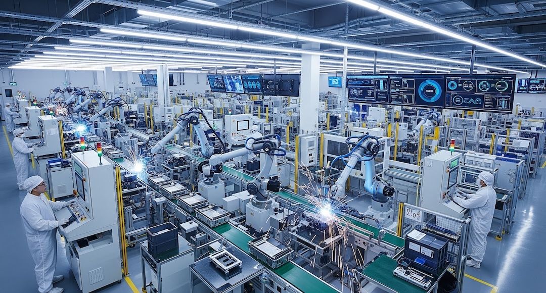
Overview
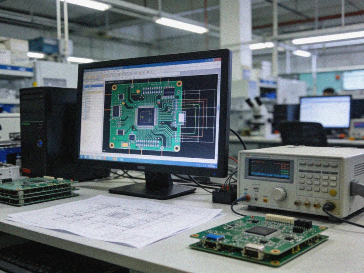
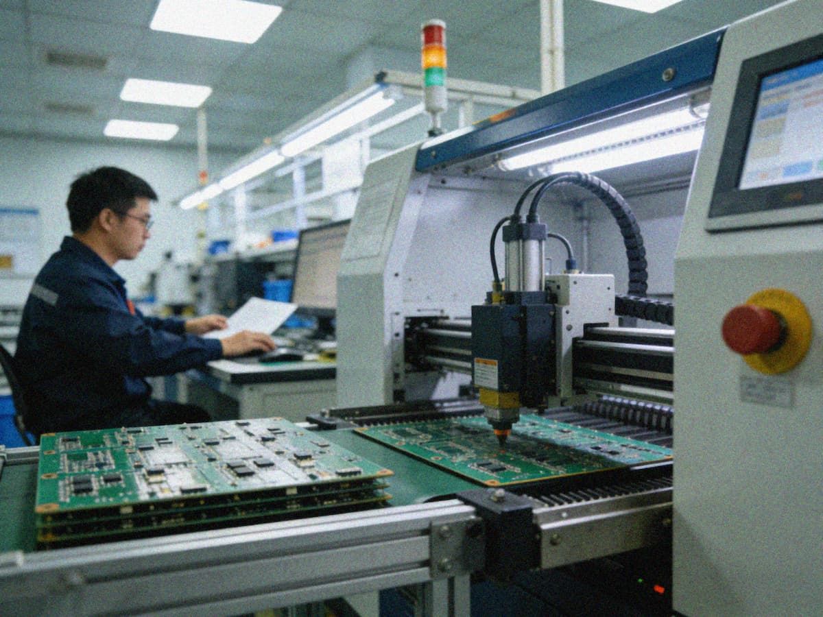
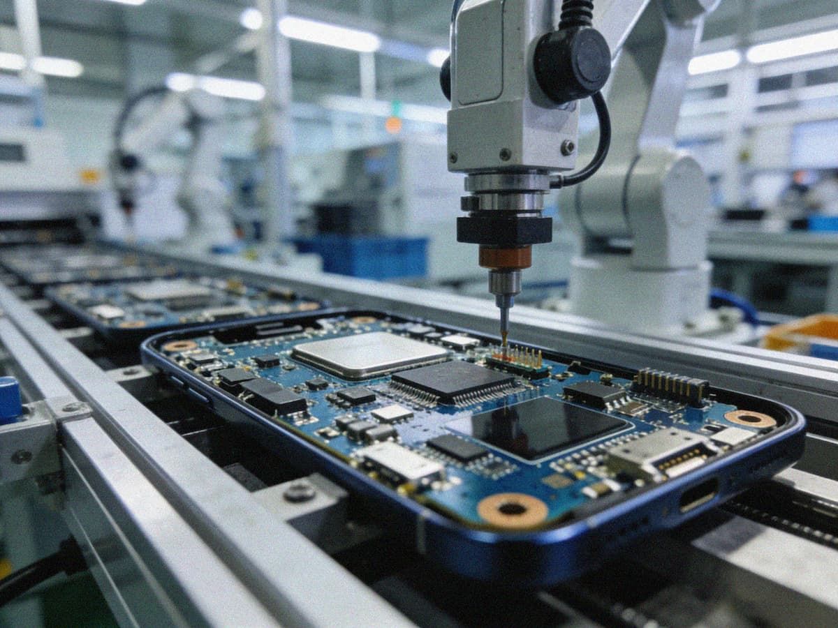
PCB design is the core link between electronic product functional planning and physical manufacturing, directly determining product performance, reliability, manufacturing cost, and time-to-market. As electronic products continue to evolve toward higher speed, higher density, miniaturization and multi-function integration, traditional PCB design can no longer meet the requirements of complex scenarios that require coexistence of high-speed signals, mixed digital-analog circuits, and specialized functional materials. Professional PCB design services cover the entire design lifecycle from schematic review to production output, integrating signal integrity simulation, DFM optimization, and structural design coordination to deliver design solutions that balance performance, cost and manufacturing feasibility for all types of electronic products.
Technical Capabilities
PCB design services cover a full range of board types and functional requirements, with core capabilities including:
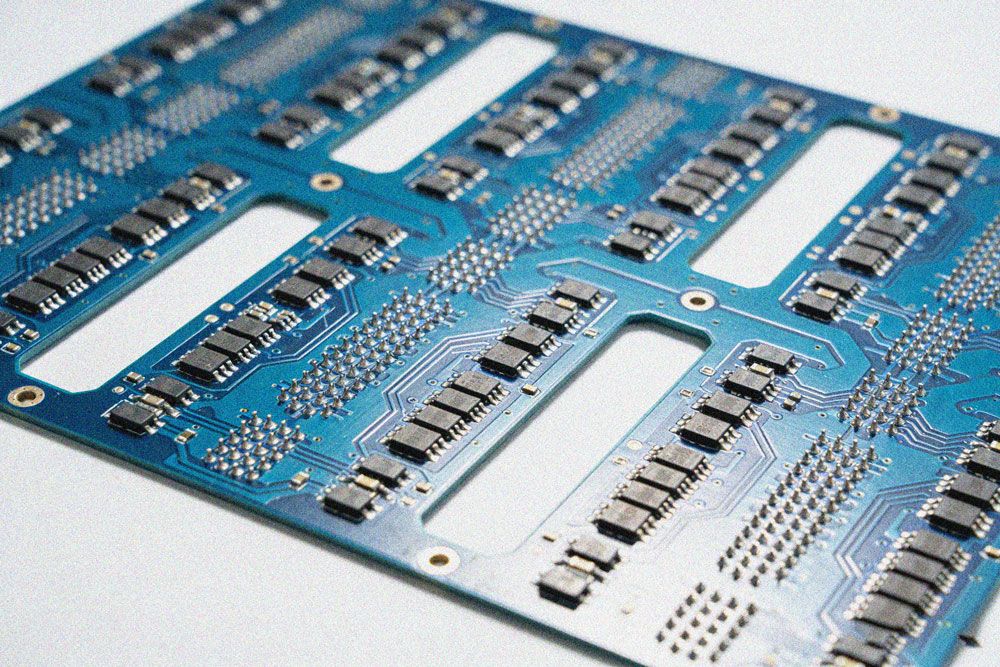
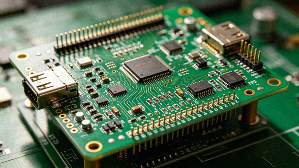
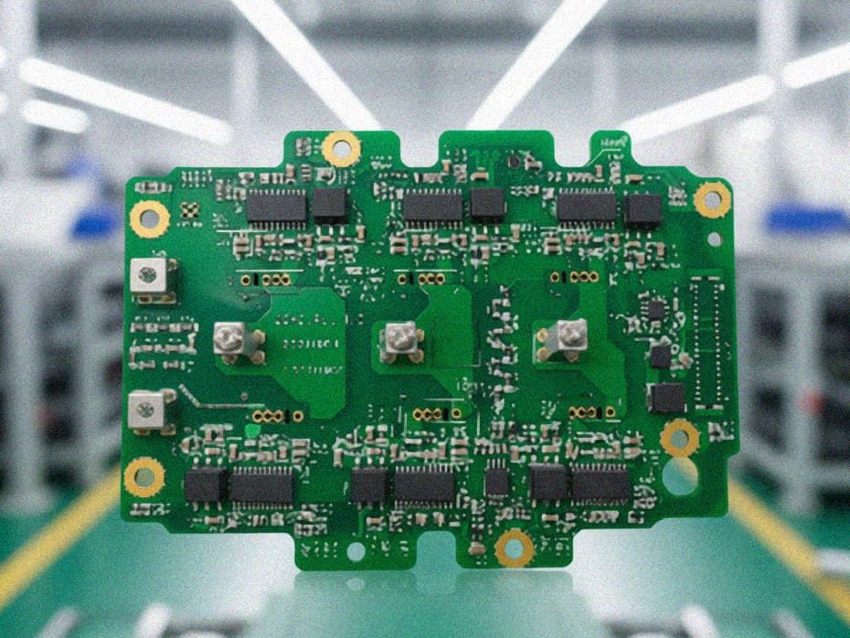
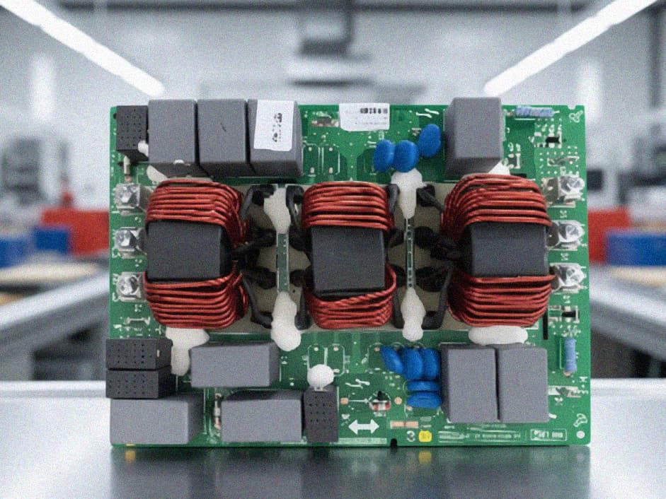
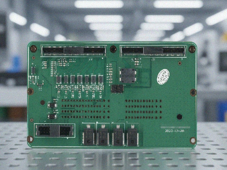
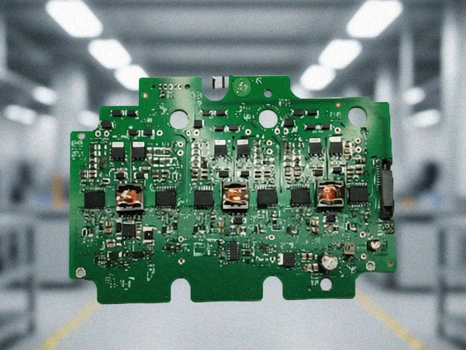
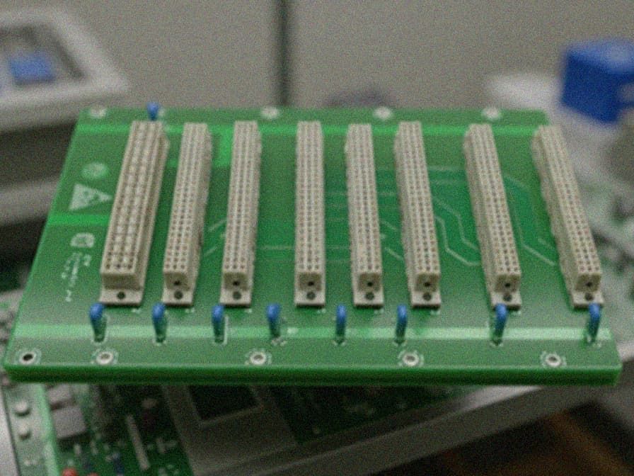
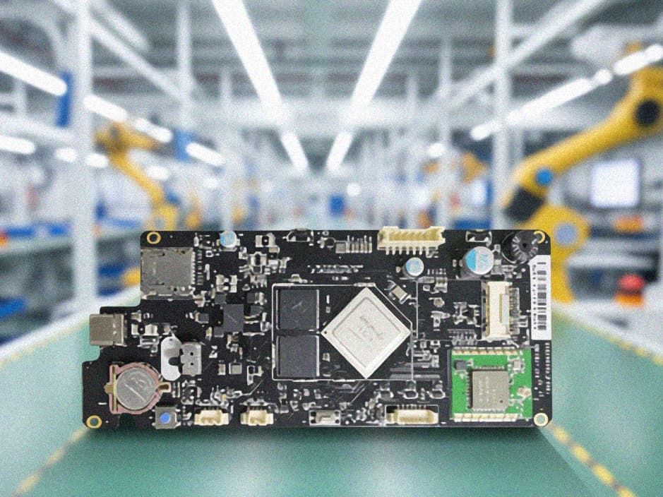
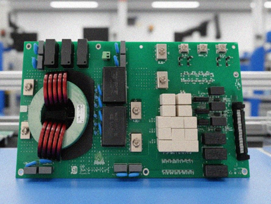
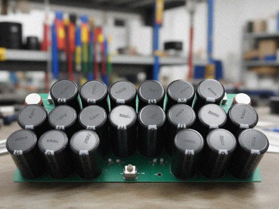
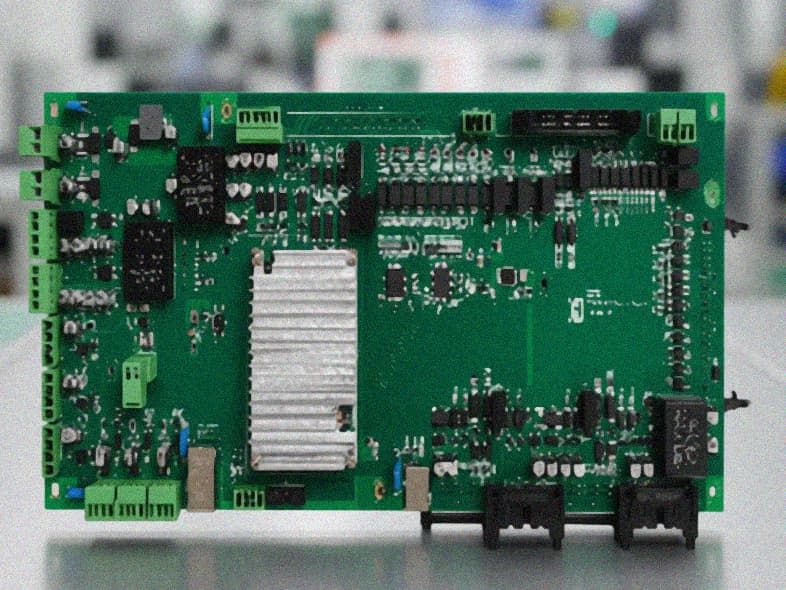
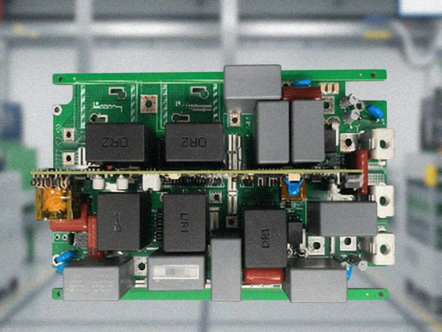
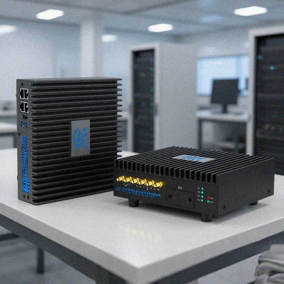
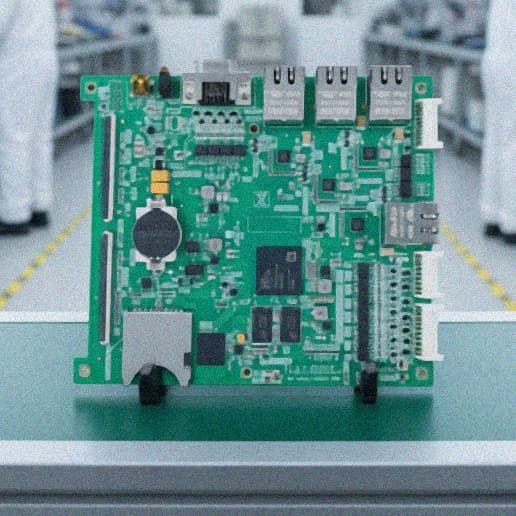
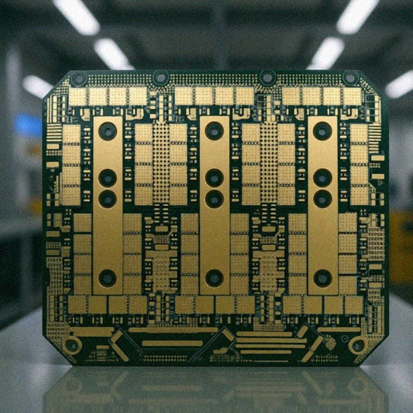
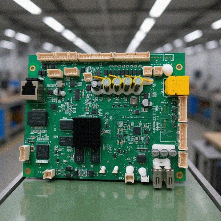
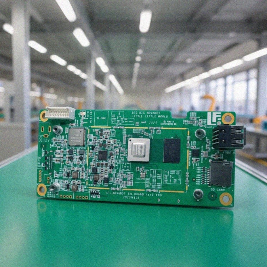
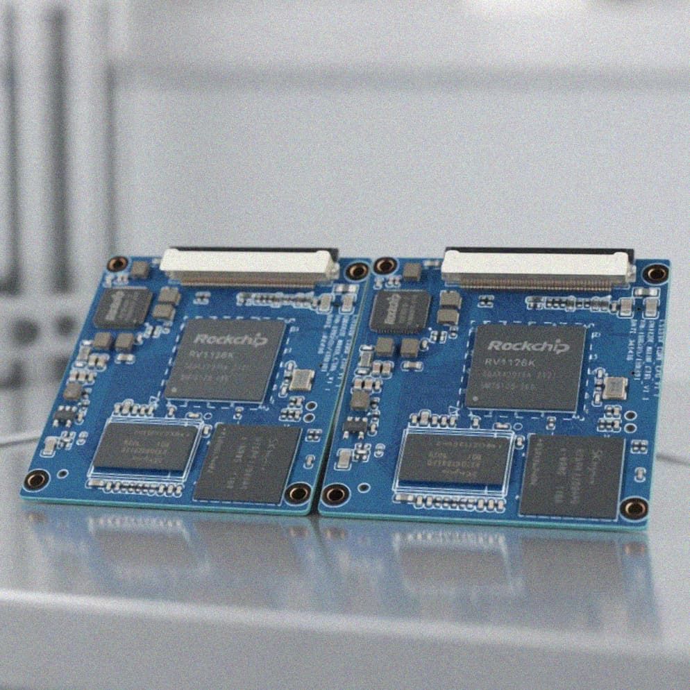
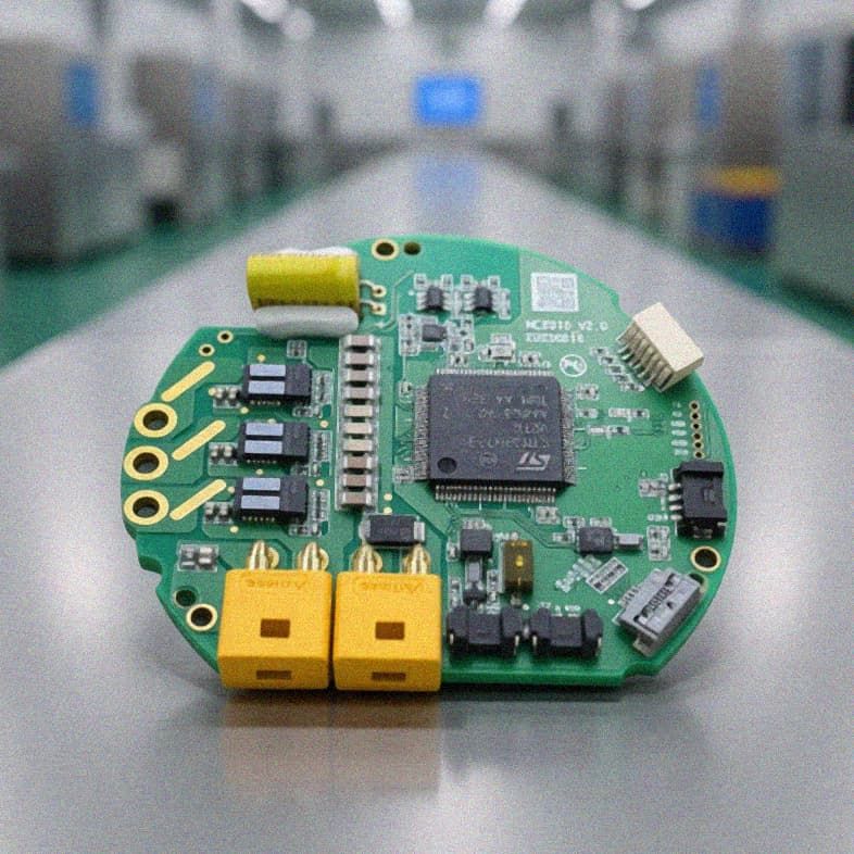
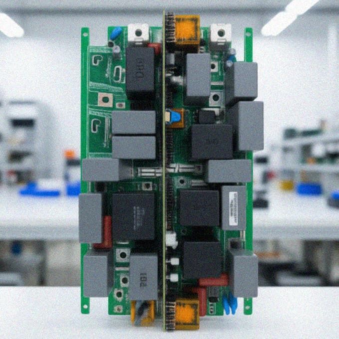
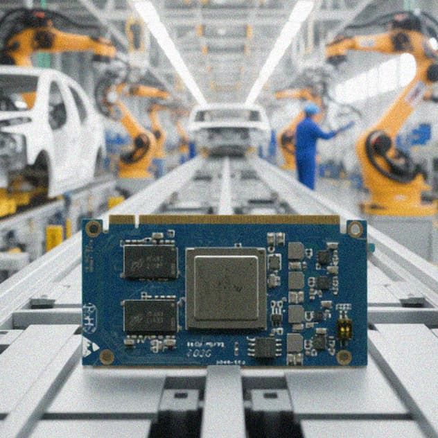
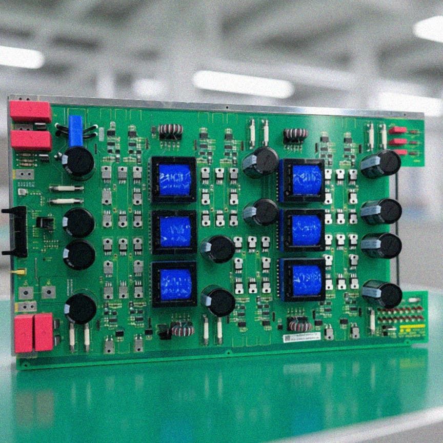
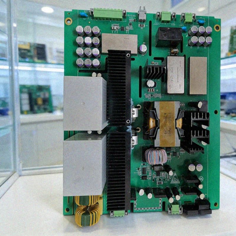
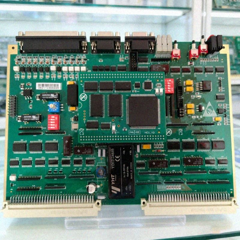
- Specialized Board Design Support: Mature design experience for almost all mainstream and niche PCB types, including embedded capacitance/resistance boards, embedded magnet boards, embedded component boards, buried copper block boards, buried ceramic boards, ceramic substrates, high-resistance carbon oil boards, backlight mini-LED boards, semi-flexible boards, IC substrates, single-sided boards, double-sided boards, multilayer boards, high-frequency step boards, HDI boards, rigid-flex boards, heavy copper boards, high-frequency hybrid boards, mechanical blind and buried via boards, metal core/metal substrate boards, high-speed backboards, and high-speed optical boards. Solutions adapt to special functional requirements of different application scenarios, from high-temperature resistance of ceramic boards to high current carrying capacity of heavy copper boards, and bending resistance of rigid-flex boards.
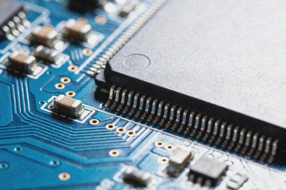
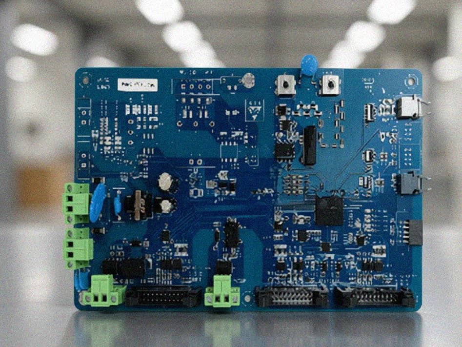
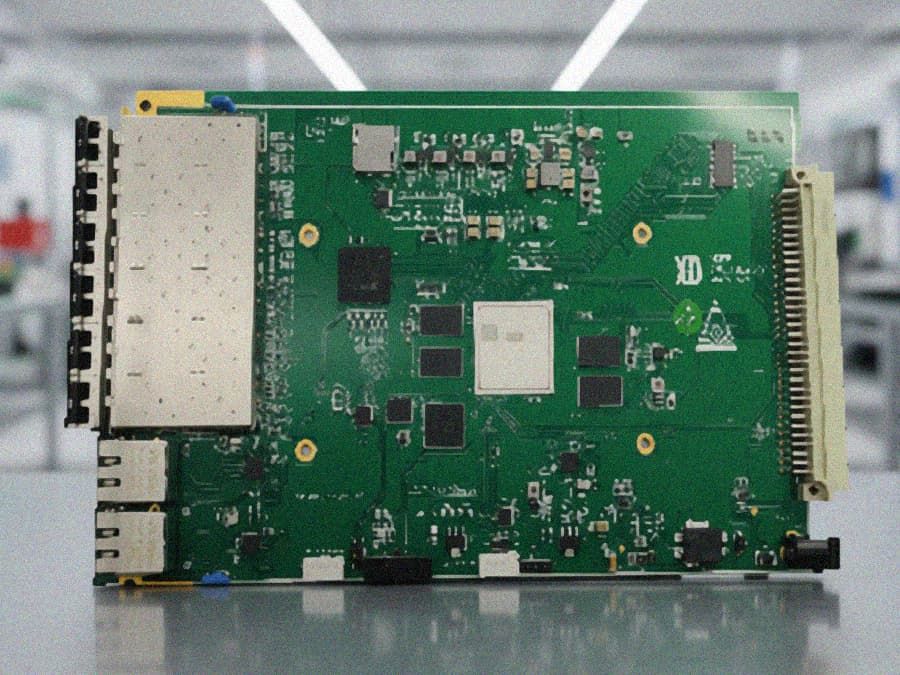
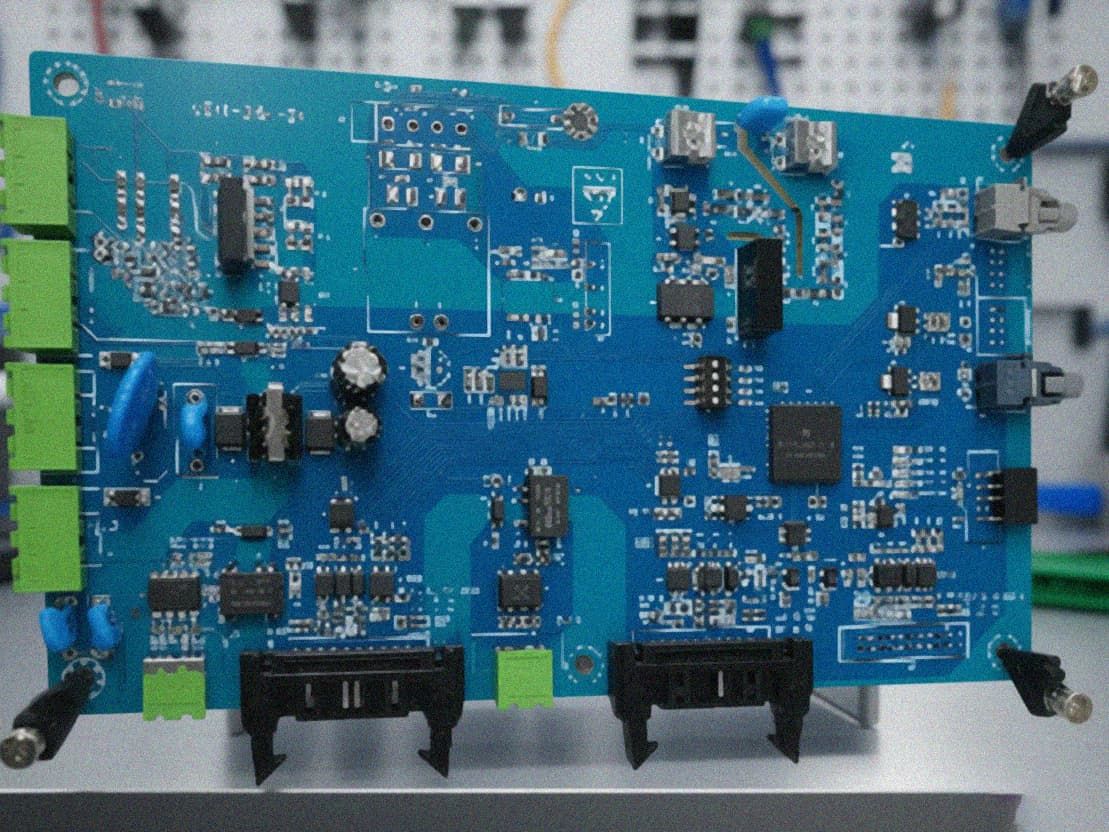
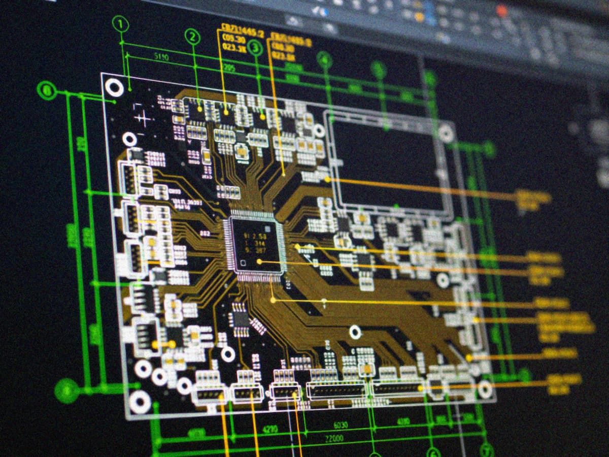
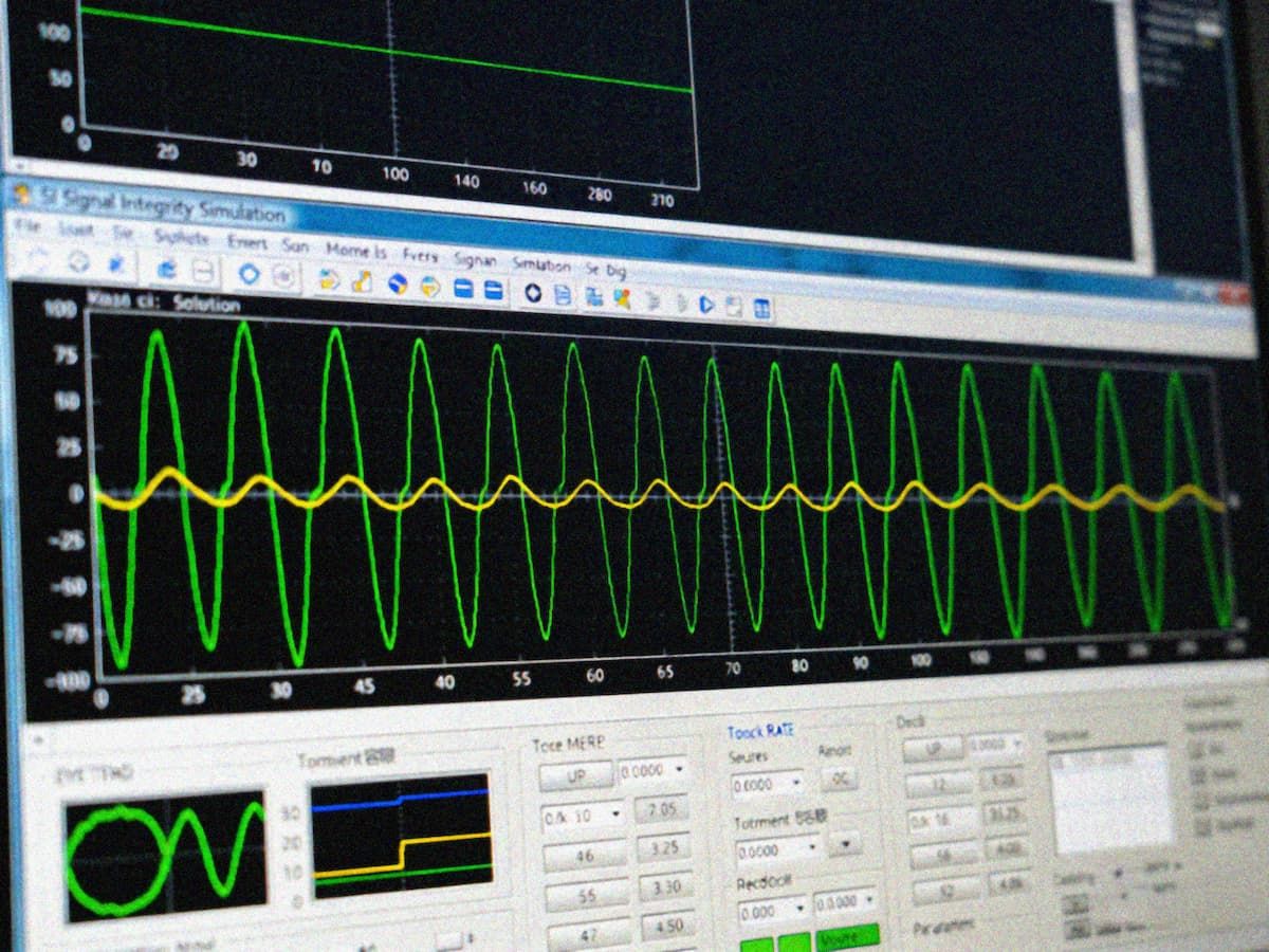
- High-Speed & Mixed Signal Design Expertise: Specialized in high-speed, high-density, mixed digital and analog PCB design, compatible with common communication interfaces including I2C, TDM, PCM, and both DC and AC power supply systems. The design process includes pre-layout signal integrity simulation, impedance matching planning, crosstalk path optimization, power noise suppression, and thermal management design, effectively reducing signal attenuation, reflection, and interference to ensure stable operation of high-speed transmission links.
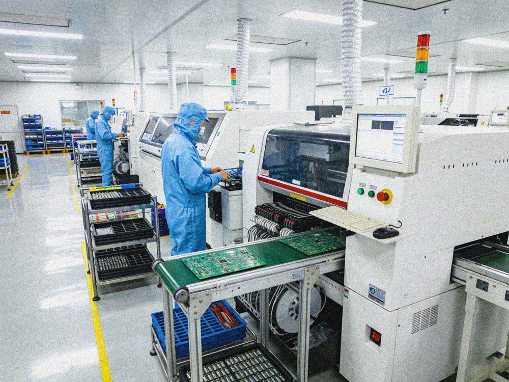
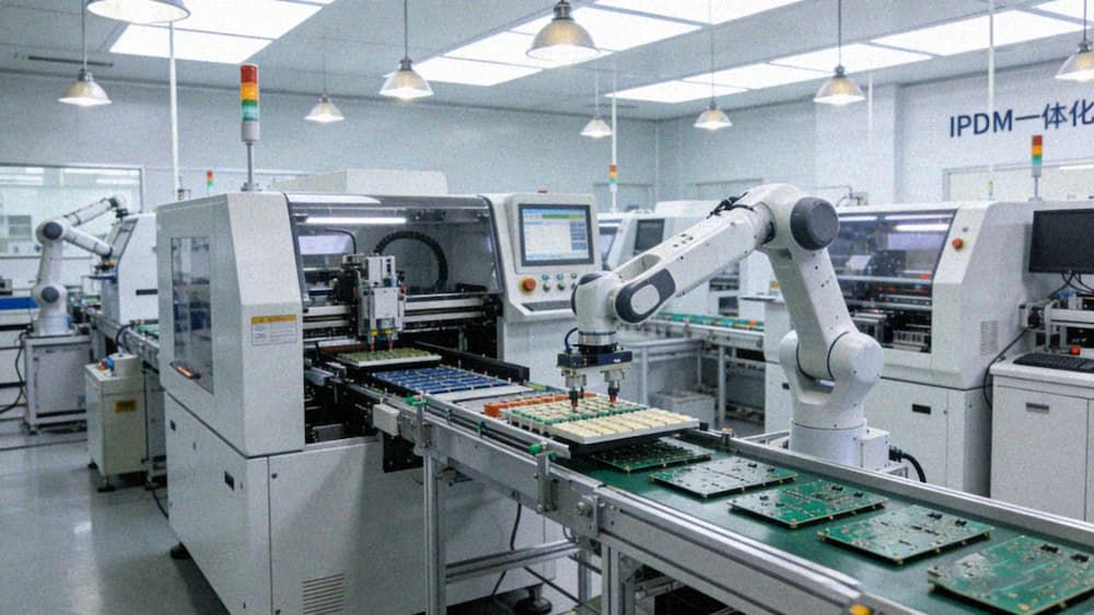
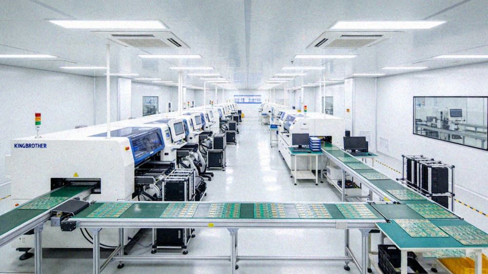
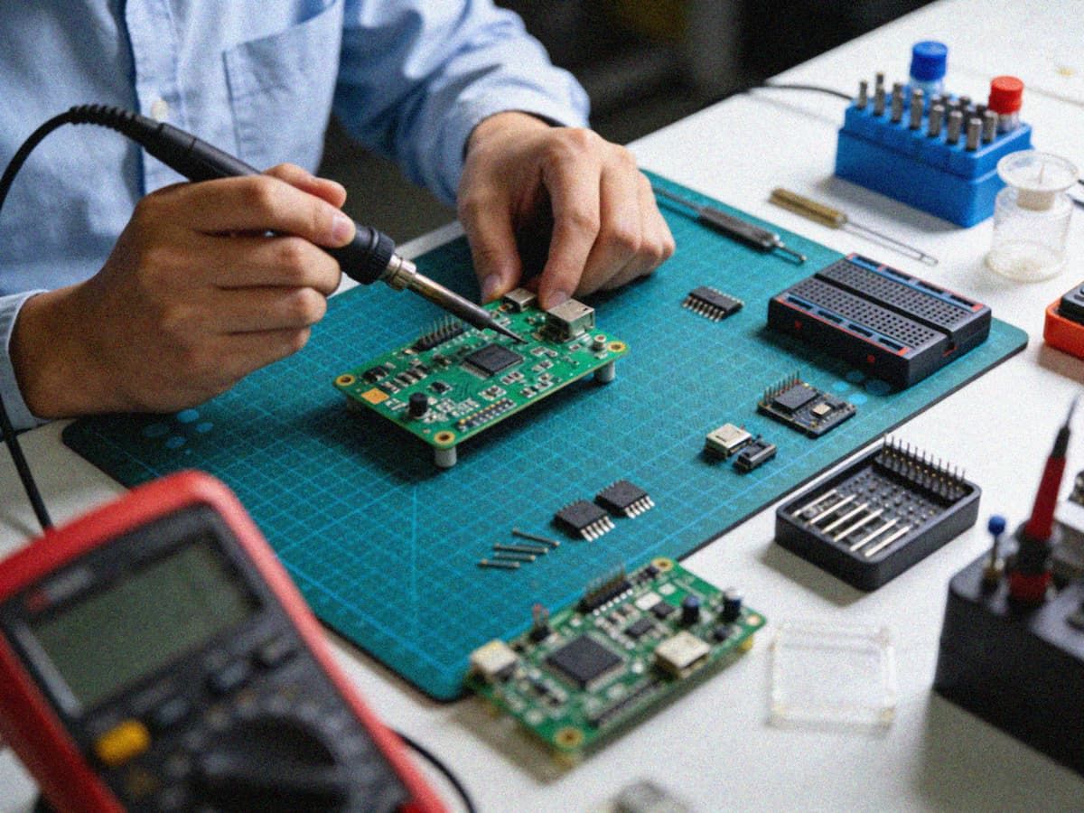
- Design Optimization & Support Services: Provide PCB design revision, training, and diagnosis services to help clients optimize existing designs, identify hidden defects, and improve internal design capabilities. The DFM (design for manufacturing) and DFA (design for assembly) audit process evaluates design solutions against actual manufacturing process capabilities, optimizing material selection, process flow, and mold opening for structural designs to reduce production defect rates, lower manufacturing costs, and shorten lead times.
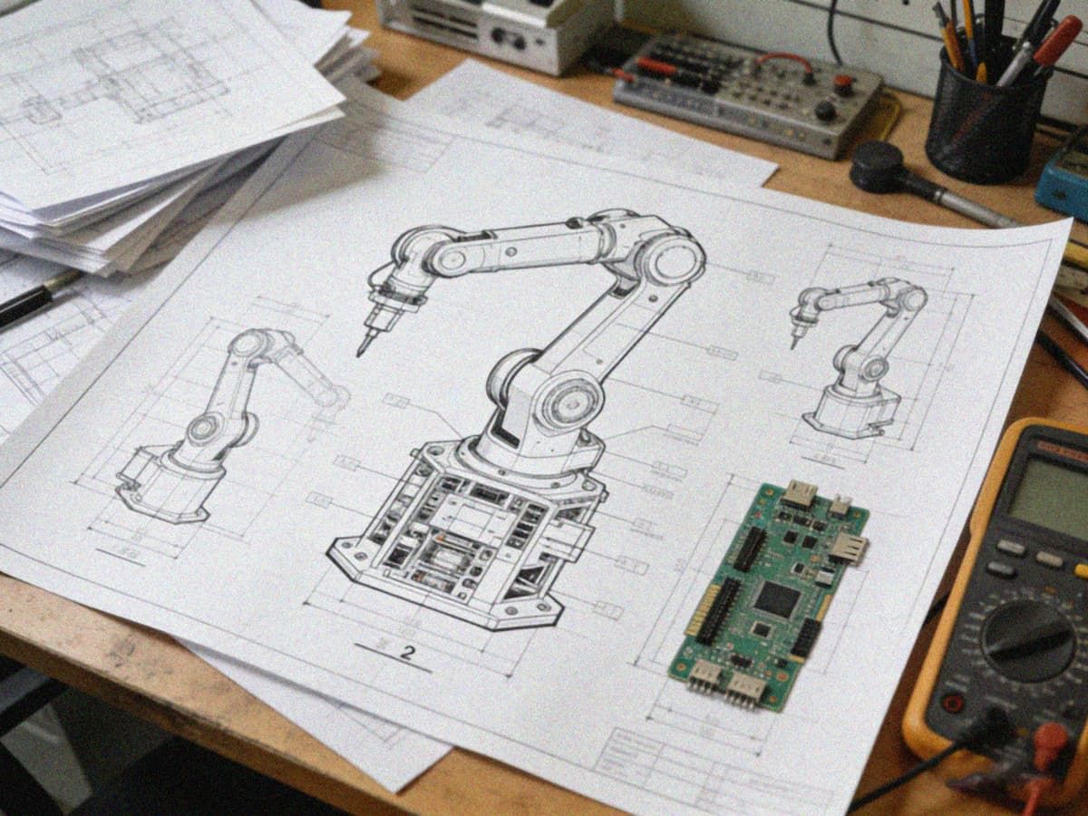
- ID & Structural Design Integration: Coordinate closely with product appearance (ID) design teams to align PCB layout with appearance style, material selection, color matching, and electromechanical coordination requirements. Structural design optimization includes reinforcement design, protective design, and process compatibility adjustment, ensuring that the PCB design fully adapts to the end product's structural and environmental performance requirements.
Quality Standards
All PCB design processes strictly follow international industry standards to ensure design reliability and manufacturing compatibility:
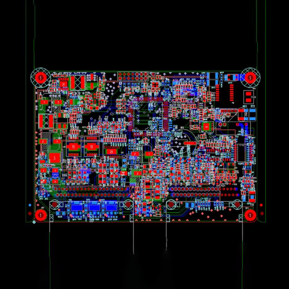
- All design outputs comply with IPC-2221 (generic standard for printed board design), IPC-2222 (rigid organic printed board design standard), IPC-7351 (surface mount design and land pattern standard) and other relevant specifications, ensuring universal compatibility with mainstream PCB manufacturing processes worldwide.
- High-speed signal path impedance control accuracy reaches ±5% tolerance, meeting the transmission requirements of high-speed differential signals, high-bandwidth memory interfaces, and high-frequency communication links, minimizing signal reflection and loss.
- All design solutions undergo multi-dimensional verification before output, including signal integrity (SI) simulation, power integrity (PI) simulation, thermal simulation, EMC pre-testing, and DFM audit, eliminating more than 95% of potential design risks before entering the manufacturing stage.
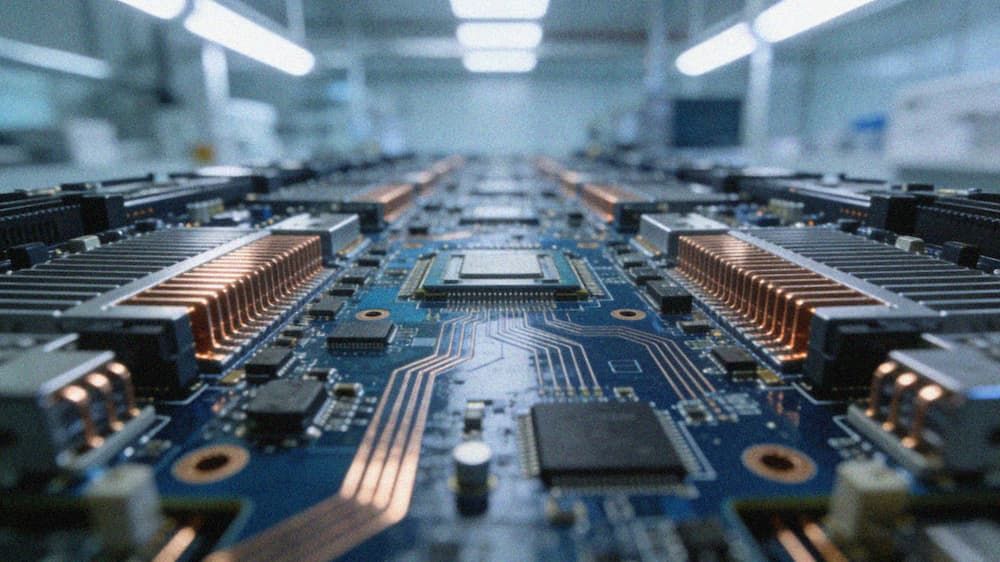
- Design outputs include complete and standardized manufacturing packages: Gerber files, BOM lists, assembly drawings, test specifications, and design specification documents, supporting seamless transition from design to prototyping, small-batch trial production, and large-scale mass production.
- All design solutions comply with RoHS, REACH, and other global environmental protection regulations, adapting to the market access requirements of different regions.
Applications
PCB design solutions are widely applicable to electronic products across all major industries, including but not limited to:
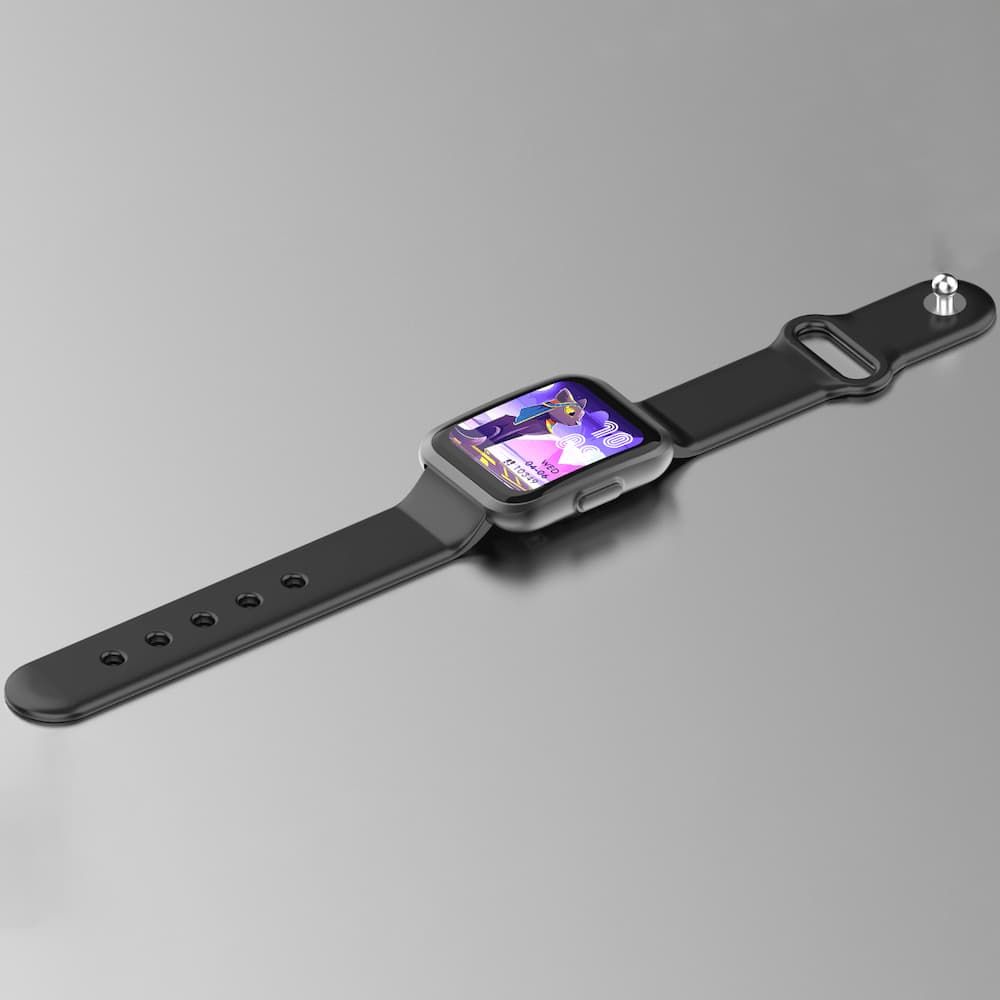
- Consumer Electronics: Smartphones, wearable devices, smart home appliances, mini-LED backlight displays, game consoles, and portable audio-visual equipment, meeting the requirements of miniaturization, low power consumption, and high functional integration.
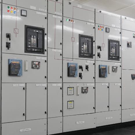
- Industrial Electronics: Industrial control systems, automation equipment, power supply units, IoT edge nodes, industrial sensors, and ruggedized handheld terminals, adapting to harsh working environments such as wide temperature ranges, high humidity, and strong electromagnetic interference.
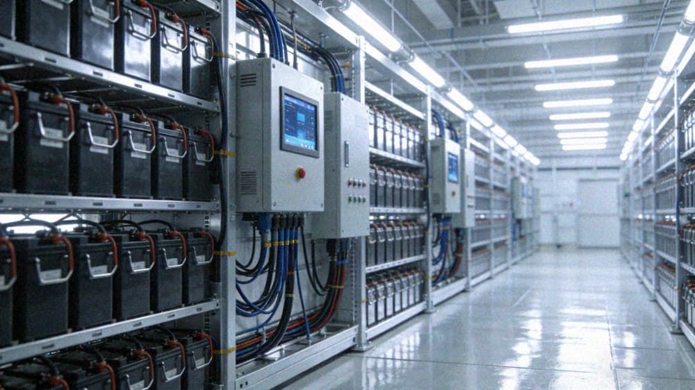
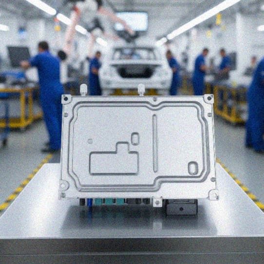
- Automotive Electronics: ADAS (advanced driver assistance systems) controllers, smart cockpit core units, battery management systems (BMS), vehicle-to-everything (V2X) communication modules, and on-board charging systems, meeting the high reliability and long service life requirements of automotive applications.
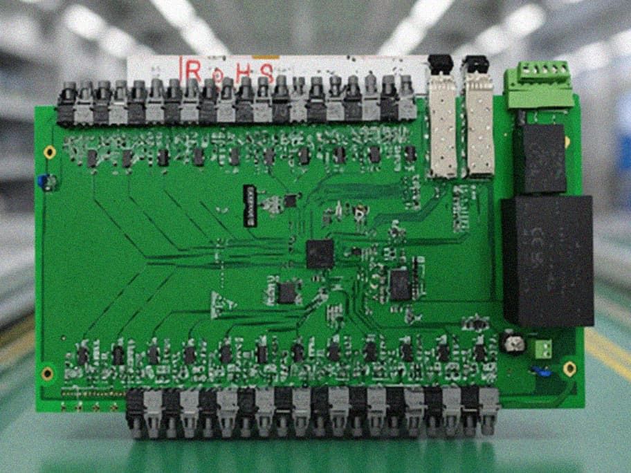
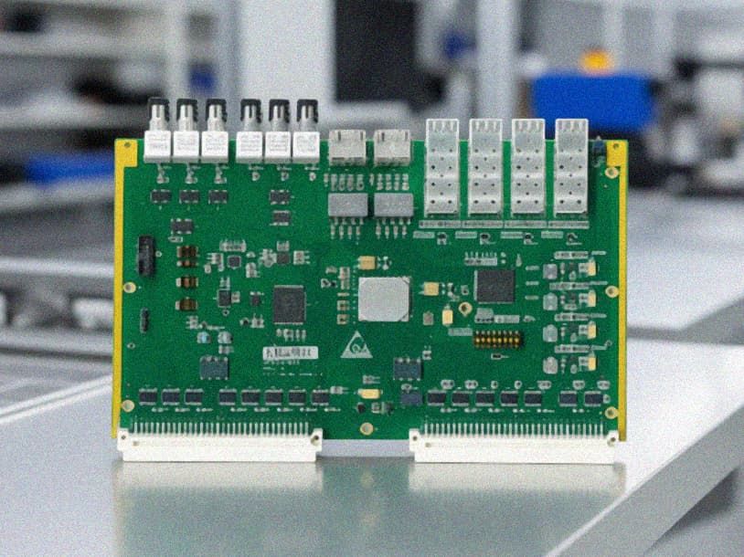
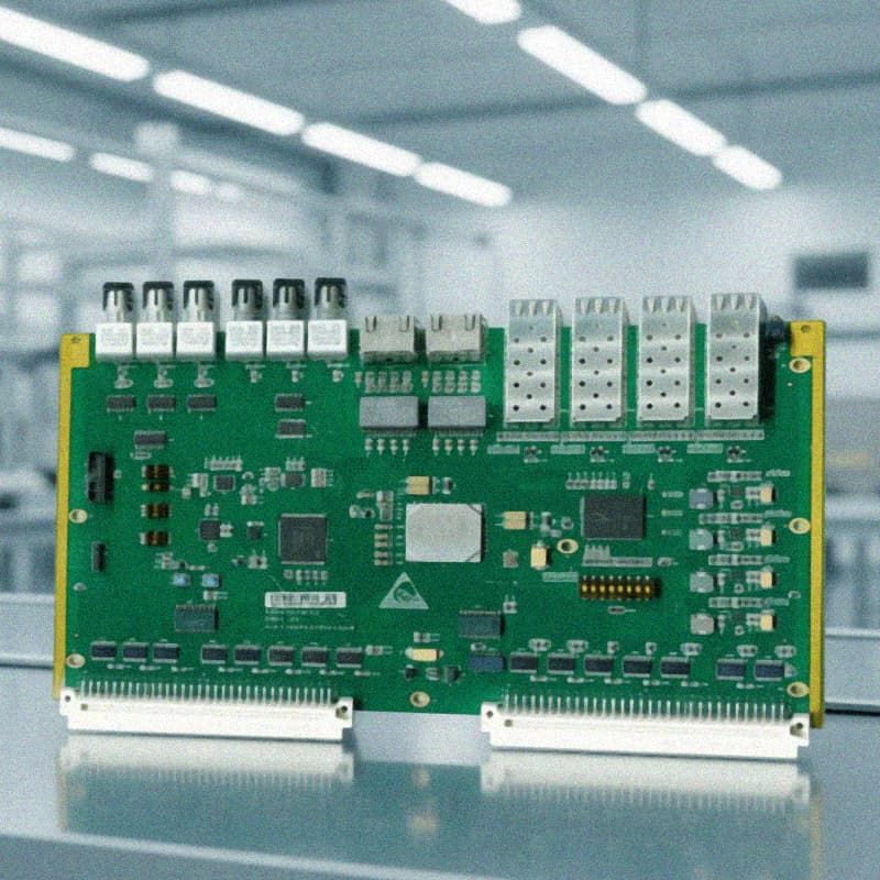
- Telecommunication Equipment: 5G base station units, high-speed routers, optical communication modules, signal transceivers, and data center high-speed backplanes, supporting high-frequency, high-speed signal transmission requirements of up to hundreds of Gbps.
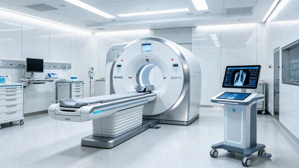
- Medical Electronics: Diagnostic imaging equipment, patient monitoring devices, portable medical instruments, and implantable medical device control units, complying with strict medical industry safety and reliability standards.
- Aerospace & Defense: Satellite communication modules, avionics systems, ruggedized military control units, and navigation equipment, meeting the requirements of extreme environmental adaptability, high anti-interference performance, and long-term stable operation.
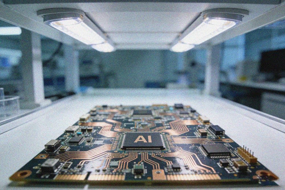
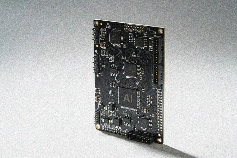
- Semiconductor Industry: IC test boards, IC substrate carrier boards, high-performance chip evaluation boards, and semiconductor manufacturing equipment control units, supporting ultra-high density routing and high-precision impedance control requirements.
Key Advantages
Professional PCB design services deliver unique value for electronic product development teams:
- Full-Cycle Design Support: Cover the entire design lifecycle from initial schematic review, stackup planning, component placement, routing optimization, simulation verification, to post-design debugging and revision support, eliminating communication gaps between design and manufacturing teams and reducing coordination costs.
- DFM-First Design Philosophy: Integrate manufacturing feasibility verification into every step of the design process, avoiding the common problem of design rework caused by incompatibility between design solutions and actual production capabilities. This reduces product development cycles by an average of 30% and lowers overall manufacturing costs by 15% to 25% compared to traditional design processes.
- Customized Solution Adaptation: No one-size-fits-all design templates are used. Tailored design strategies are developed based on your product's specific application scenario, performance indicators, size constraints, and budget requirements, whether you are developing a high-frequency 5G communication product, a high-current industrial power supply, or a miniaturized wearable device.
- Continuous Technical Support: In addition to delivering design outputs, professional PCB design training and diagnostic services are provided for your in-house design team, helping you identify hidden defects in existing designs, optimize internal design workflows, and improve overall design maturity to support long-term product development plans.
Contact Information
If you have any PCB design requirements for specialized board types, high-speed signal products, mass production optimization, or design capability improvement, please reach out to our technical team. We will provide you with free design feasibility evaluation, customized solution suggestions, and professional technical consulting services to help you accelerate product launch, reduce development costs, and improve product market competitiveness.