When we talk about smart cities, industrial inspection, or unmanned delivery vehicles, we're actually talking about countless "intelligent terminals" deployed at the edge of the scene. These devices are called Edge AI Devices. Unlike cloud servers with near-limitless computing power and space, they must process massive amounts of data and make decisions in real time within harsh field environments, with limited size and power consumption. The core challenge largely lies in the printed circuit board (PCB) that houses their "brain."
As a supplier that has long served AI hardware innovation, we deeply understand that a successful edge AI device PCB is far more than simply connecting chips and components. It's a precise balance of power consumption, density, heat dissipation, and signal integrity on a millimeter-square battlefield.
The "Extreme" Requirements of Edge AI Accelerators on PCBs
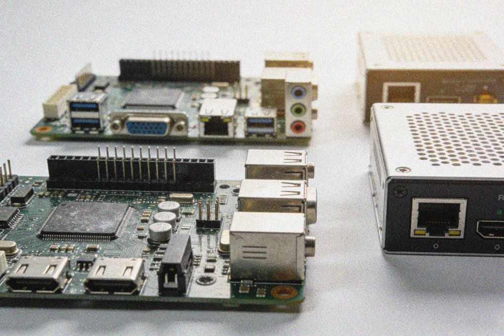
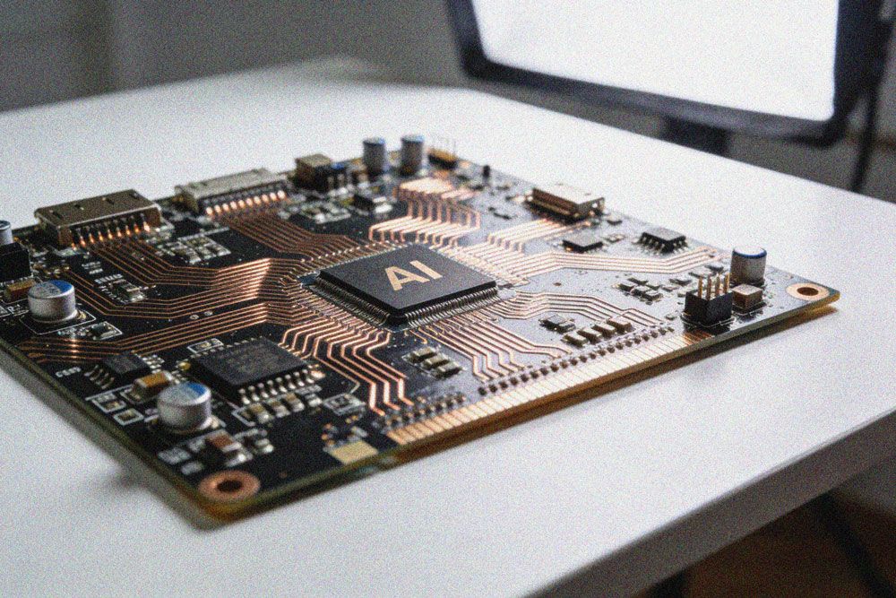
Take current mainstream Edge AI Accelerator modules, such as the NVIDIA Jetson series, as an example. They encapsulate powerful AI computing power in a palm-sized module. For example, the Jetson Orin NX offers up to 100 TOPS of AI computing power and can handle 18 1080p video streams. However, this high performance also brings design challenges: high-speed signal interfaces (such as MIPI CSI-2 and PCIe) have extremely high transmission rates and are highly sensitive to signal integrity; at the same time, power consumption of up to tens of watts can generate significant heat in a confined space.
These challenges directly translate into stringent requirements for PCB design. Based on our project experience, PCBs serving such applications often need to have the following characteristics:
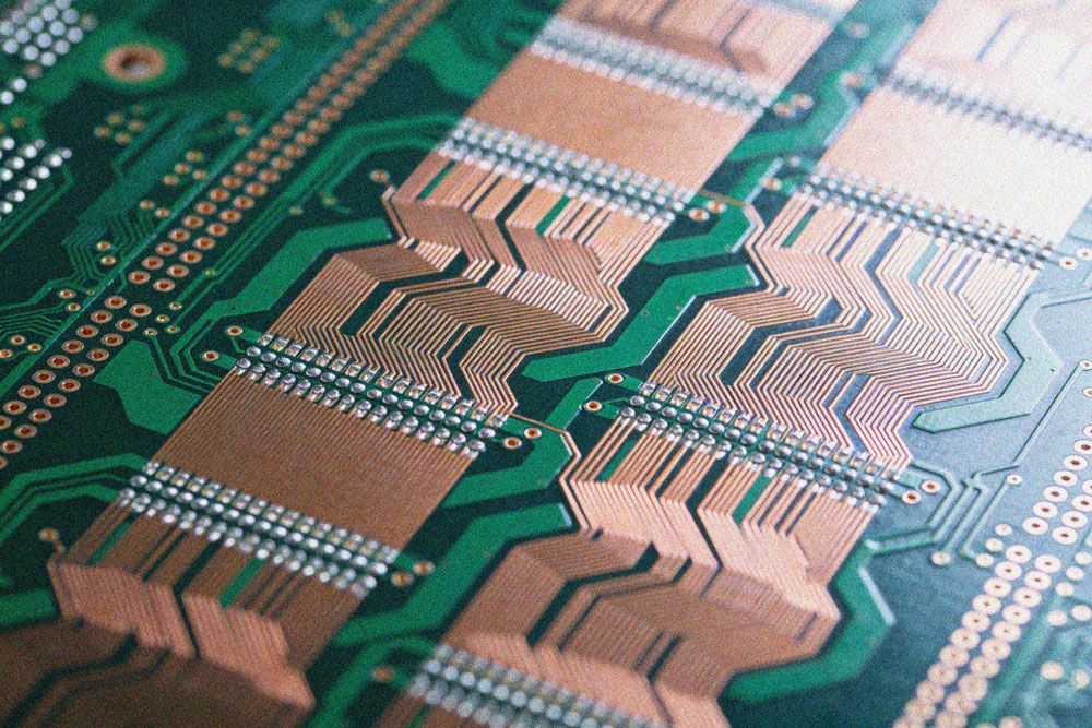
High multilayer structure: To route all high-speed signal lines and ensure power integrity within a limited area, the number of layers on the board typically needs to reach 16 or even 32.
Extremely fine wiring: To achieve high-density interconnects, the inner layer trace width and spacing need to be 4.5/2.5 mil (approximately 0.114/0.064 mm), which poses a significant challenge to manufacturing etching precision.
Miniaturized Drilling: With increasingly smaller component pin pitches, the minimum mechanical drilling diameter for PCBs needs to reach 0.2mm or even smaller.
Specialty Materials: To ensure low-loss transmission of high-speed signals, high-speed materials like TU933+ are often used, with optimized dielectric constants and loss factors.
Design Practices Behind Low Power Consumption and High Density
Parameters are just the goal; how to achieve them is key. In multiple edge AI device projects, we encountered several typical problems and developed corresponding design and manufacturing solutions.
First is impedance control and signal integrity. A motherboard for an edge device used in AI vision may have a MIPI interface rate exceeding 10Gbps. Any tiny impedance discontinuity can cause signal reflection and attenuation, resulting in image data errors. Our approach is to perform precise layer stack-up planning and simulation during the design phase. For example, in a 10-layer board design, we strictly control the characteristic impedance of key differential pairs to 100 ohms, achieving this by adjusting dielectric thickness, trace width, and copper thickness. Our self-developed KBEDA SKILL design tool integrates over 400 functions, enabling simulation and prediction of signal reflections, crosstalk, and delays during the placement and routing phase, thus mitigating risks in advance.
Secondly, stable and efficient power supply design is crucial. Edge AI accelerator modules have a large dynamic range of power consumption, and instantaneous current can be very high. An unclean power supply can directly lead to chip instability or performance degradation. Our design strategy employs multi-layered ground and power planes to provide low-impedance return paths. For example, in the core power supply area, we arrange the power plane and ground plane closely adjacent to each other and add a decoupling capacitor network. In some high-end designs, we also introduce power monitoring and management modules to balance the power supply of each phase in real time, minimizing power supply noise.
Finally, and most importantly, is thermal management. Power consumption means heat generation. In a sealed outdoor edge computing box, if heat cannot be dissipated in time, the chip will throttle due to overheating or even be damaged. The PCB itself can become part of the heat dissipation system. We consider using high thermal conductivity dielectric materials in the PCB stack-up or designing large areas of exposed copper on the back of the chip, conducting heat to the heat sink via via arrays. For modules like the Jetson AGX Orin with power consumption reaching 30-40W, we even integrate heat pipes or vapor chambers on the PCB to ensure long-term stable operation within an industrial-grade temperature range of -20°C to 60°C.
For device developers, finding reliable AI edge device PCB suppliers means focusing more on algorithms and applications, rather than the details of hardware implementation. This requires suppliers to have a closed-loop capability across the entire design and manufacturing chain.
On the design side, a deep understanding of the characteristics and requirements of different AI chip platforms such as ARM, GPU, and FPGA is necessary. We have provided complete hardware design solutions for multi-functional monitors and industrial controllers based on platforms such as RK3568 and NXP i.MX 8M Plus. This encompasses not only schematic and PCB design, but also driver development, system porting, and even EMC design and optimization for complex environments.
On the manufacturing side, high-density design must be matched with high-precision processes. Our multi-drilling technology effectively reduces stubs on high-speed signal channels, improving signal quality; resin-filled high-density vias provide a flat base for surface mounts, preventing solder joint defects. For special structures such as metallized slots and crimp holes, we have mature precision control solutions to ensure reliable connector interconnection.
A concrete example comes from a humanoid robot project we served. The customer's infrared camera control system needed to achieve real-time image processing in environments with high vibration and strong electromagnetic interference. We selected the RV1126 chip, specifically designed for AI vision, as the core, and adopted automotive-grade design principles and a composite heat dissipation system in the PCB design. By optimizing the power architecture and sensor interface layout, and using high-TG materials, we ultimately achieved high-reliability operation of the system in harsh environments, accelerating the mass production process of the customer's products.
Another case study of an intelligent environmental controller demonstrates the value of low-power design. In agricultural and livestock farming scenarios, equipment needs to operate in high-temperature, high-humidity, and even corrosive environments year-round. We enhance the corrosion resistance of the PCB by using a high-TG substrate with a Tg ≥ 170°C combined with immersion gold surface treatment. Simultaneously, in the PCBA stage, we employ a three-proof coating process and strong/weak current isolation design, significantly reducing the failure rate of the entire machine in corrosive environments and lowering maintenance costs for farmers.
The innovation of edge AI devices, on the surface, is the evolution of algorithms and software, but at its core, it is the continuous advancement of hardware engineering, especially PCB design capabilities. Low power consumption and high density—two seemingly contradictory goals—are being unified through more refined design, more advanced materials, and more reliable processes.
As fellow innovators in smart terminals, we firmly believe that an excellent PCB is the physical foundation for fully unleashing the powerful computing power of edge AI accelerators. It works silently, yet determines whether smart terminals can operate stably, efficiently, and sustainably in the real world. In the future, as AI penetrates more edge and microscopic scenarios, the requirements for PCB design will only increase. We have accumulated enough practical parameters and solutions along this path and are ready to meet the next challenge.
Need Support for Edge AI Hardware Development?
We provide:
- Jetson / Rockchip carrier board design
- High-speed interface layout (MIPI / PCIe / USB3.0)
- Thermal simulation & heatsink integration
- Low-power PDN optimization
- Prototype to mass production