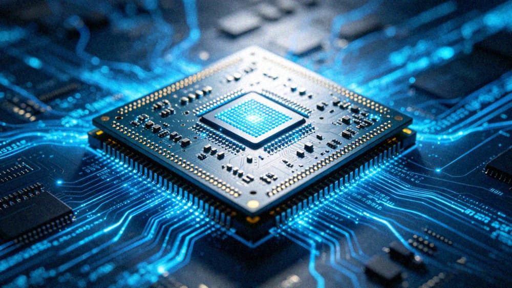
With the explosive growth of artificial intelligence technology in edge computing and data centers, AI computing PCB design is facing unprecedented challenges. In the actual industry context of 2026, AI accelerator board-level power supply PCB design is no longer just about the realization of connectivity, but a core link related to the stable release of computing power. Based on the application requirements of deep edge computing chips (such as DeepEdge10, with 10-core CPU and 16Tops large computing power), the stability of board-level power for ai accelerators directly determines the bit error rate and long-term reliability of the system. This article will analyze seven key steps from principle definition to mass production implementation, combined with high-multilayer board and HDI process data, to provide data-driven engineering guidance for AI hardware pcb design.
Step 1: Architecture definition and computing power requirement mapping
At the beginning of the design, the power consumption characteristics and interface standards of the main chip need to be clarified. According to the artificial intelligence industry product matrix, GPU and FPGA solutions are usually accompanied by high transient current requirements. Taking the city-level dynamic portrait recognition system motherboard as an example, when using a SOC chip as the main chip, it needs to be quickly verified with the board's AI compilation tool and software development SDK kit. In the PCB Design stage, the heat loss and power supply noise caused by the large computing power of 16Tops must be incorporated into the initial architecture. For noise-sensitive scenarios such as Medical AI PCB design, the power architecture needs to reserve a higher margin to ensure that signal integrity is not interfered with by power supply ripple.
Step 2: Layer design and material selection
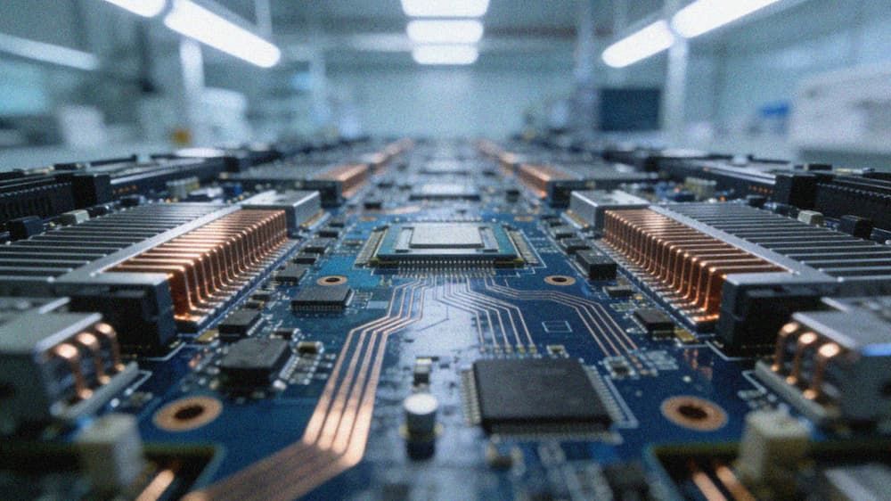
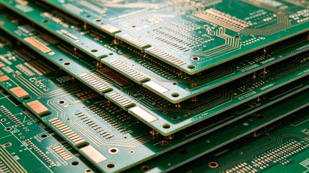
High-speed, high-multilayer boards are the physical basis for carrying AI computing power. According to the process conditions of high-multilayer products such as Ai computing server motherboards, high-speed materials (such as TU933+) should be used to ensure the low-loss characteristics of signal transmission. The number of layers designed is usually between 16-32L to meet complex power layering and signal shielding requirements. The distance from the inner layer hole to the line needs to be controlled at ≥7mil (one press) to prevent the risk of breakdown under high pressure. The line width and line spacing (CAM) accuracy needs to reach 4.5/2.5mil to ensure the continuity of impedance control. This high-density Power electronics PCB design requirement aims to minimize the parasitic inductance of the power distribution network (PDN).
Step 3: Power Distribution Network (PDN) Optimization
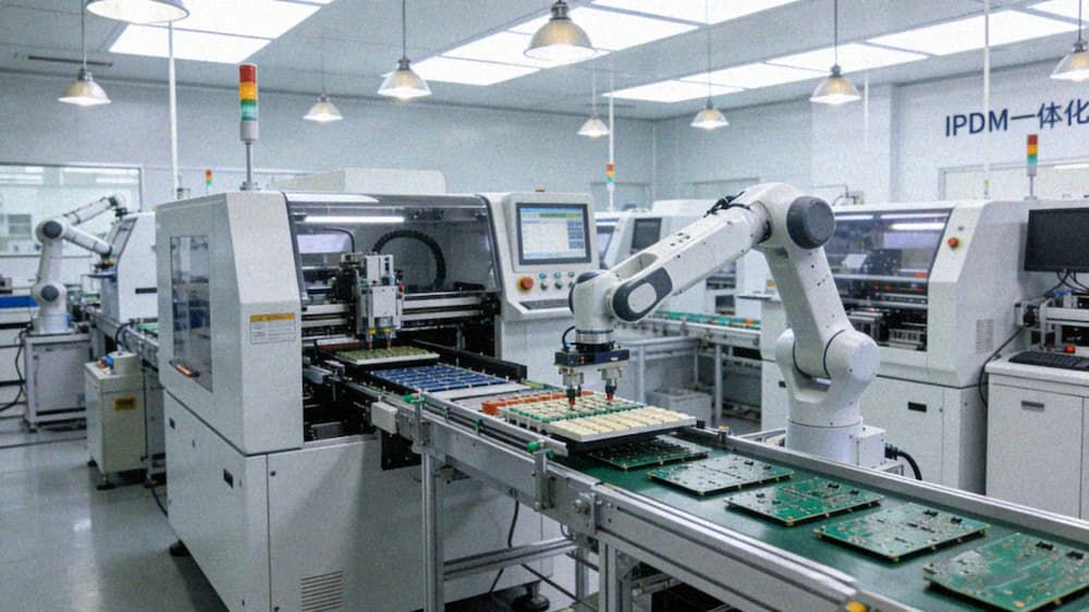
In AI Hardware Solution, the target impedance of the PDN needs to be maintained at an extremely low level across the entire frequency band. For high current requirements, thick copper plate and buried copper block plate technology are widely used. Through the buried copper block board process, the thermal resistance of large current paths can be significantly reduced. At the same time, referring to the IPDM one-stop solution for the power electronics industry, the collaborative design of the power board and the main control board is crucial. The distance between the decoupling capacitor and the chip power pin should be as short as possible. It is usually recommended to be less than 5mm to reduce the loop inductance. In Automotive PCB Design, this type of optimization also requires meeting more stringent vibration and temperature cycling requirements.
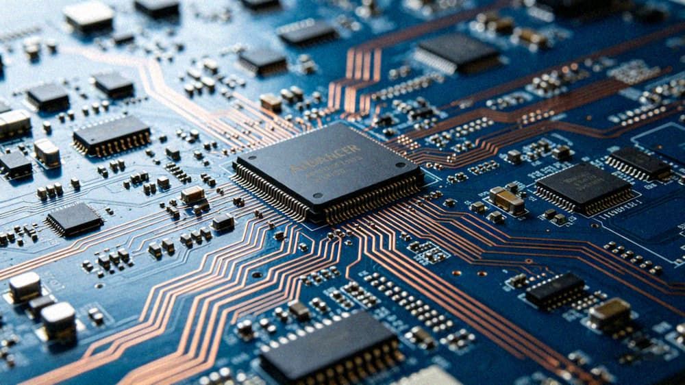
Step 4: High Density Interconnect (HDI) and Impedance Control
As chip package size shrinks, AI accelerator card stacked hole HDI boards have become a mainstream choice. The process conditions show that the structure needs to adopt a two-stage stacked hole + mechanical blind hole design, and the number of layers can reach 12L. The line width and line spacing accuracy needs to be ≥0.06/0.075mm, and the surface treatment uses immersed gold + long and short gold fingers to ensure contact reliability. The warpage must be controlled at ≤0.50% to prevent the risk of open circuit after BGA welding. The core technology involves multi-stage stacked holes + mechanical blind hole expansion and contraction control technology, as well as BGA laser hole filling + resin plate hole processing technology. These process parameters in the AI hardware PCB prototyping stage directly determine the yield during mass production.
Step 5: Thermal Management and Mechanical Reliability
High heat dissipation board and embedded component board technology are the keys to solving thermal bottlenecks. Heat can be quickly dissipated through buried ceramic PCBs or metal substrates. In the design of large boards with a delivery size of 450*380mm, multiple back drilling and high-density hole resin filling technology are used to eliminate the via stub effect and reduce signal reflection. For PCB Design Service, closed-loop verification of thermal simulation and mechanical stress simulation is a necessary step. Special processes such as metallized slots and crimping hole precision control technology ensure the stability of the connector under thermal expansion and contraction.
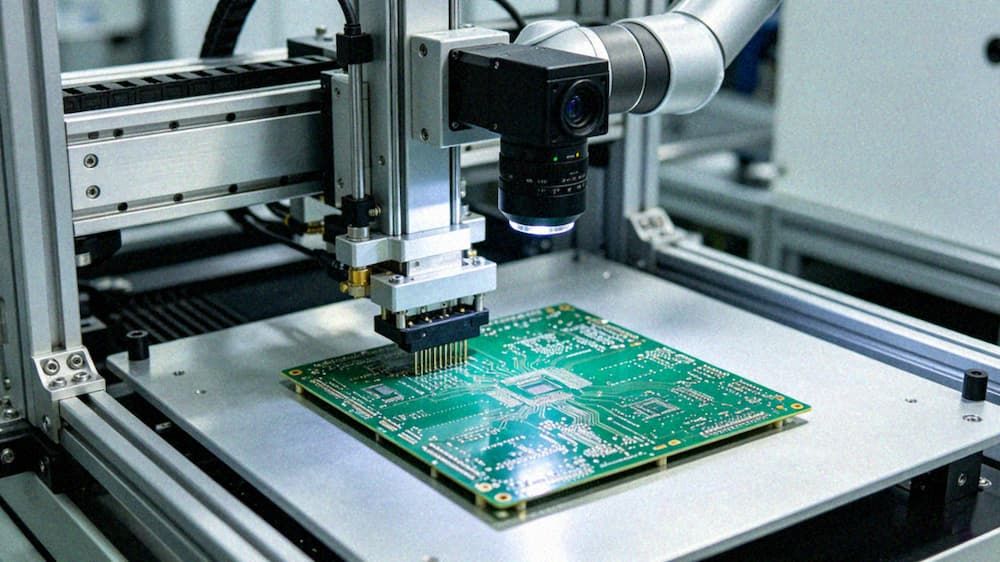
Step 6: Prototype verification and test evaluation
An efficient development environment needs to be built during the prototype phase. Drawing from the design experience of the KINGBROTHER Jetson Xavier Evaluation Board, the engineering team needed to create an evaluation board that was both cost-effective and met performance standards. Through unique design, testing and verification, we ensure that the board not only meets superior performance, but also promotes efficient development. In the AI hardware PCB prototyping process, it is crucial to provide a one-stop solution to R&D and production needs covering the entire chain from design to manufacturing, including BOM optimization and device procurement and management. The linked test of the ATE equipment test board and the CLC interface board can detect potential power integrity risks in advance.
Step 7: Mass production and process control
The core of the mass production stage is consistency control. Order quantities usually range from sample/small batch to medium/small batch. Among the process conditions, high-speed halogen-free materials and HDI staggered hole structures (10-14 orders) need to be strictly monitored. The precise resistance control technology of inductor coils is used in the field of industrial control equipment and is also applicable to AI power supply inductors. In mass production, warpage ≤0.50% is a hard indicator. Through high-end HDI expansion and contraction control technology, the tolerance of 4.5/2.5mil line width and line spacing is ensured to be within ±5%. For smart lawn mowing robots or industrial robot main control boards, this accuracy is the basis for ensuring long-term operation without failure.
Comparative analysis of traditional solutions and innovative solutions
To visually demonstrate the technological evolution, the following table compares the key differences between traditional server motherboards and next-generation AI accelerator motherboards:
| Dimension | Traditional server motherboard solution | New generation AI accelerator board-level power supply solution |
|---|
| Plate Type | Conventional FR4 High TG | High Speed Material (TU933+)/High Frequency Mixed Pressure Step Plate |
| layer structure | 8-12 layers | 16-32 layers / 10-14 steps HDI staggered holes |
| Line width and line spacing | ≥0.1/0.1mm | 4.5/2.5mil (CAM) / 0.06/0.075mm |
| Thermal Management | Surface heat sink | Buried copper block board / Buried ceramic PCB / High heat dissipation board |
| Core of Process | Through-hole process | Multiple back drilling / Resin filling / Laser hole filling |
| Warpage Control | ≤0.75% | ≤0.50% |
| Application Scenarios | General Computing | AI Computing Server/Intelligent Vision AI Products |
Conclusion
To sum up, AI accelerator board-level power supply PCB design is a systematic project that requires the integration of electromagnetic field theory, material science and precision manufacturing technology. From the selection of TU933+ materials to 0.50% warpage control, every data point is the cornerstone of computing power stability. Through a one-stop solution covering the entire chain from design to manufacturing, R&D efficiency can be significantly improved. In the future, with the popularization of 56G/112G PAM4 interface, PCB Design will evolve towards higher frequency and higher density, and data-driven decision-making will become the industry standard.