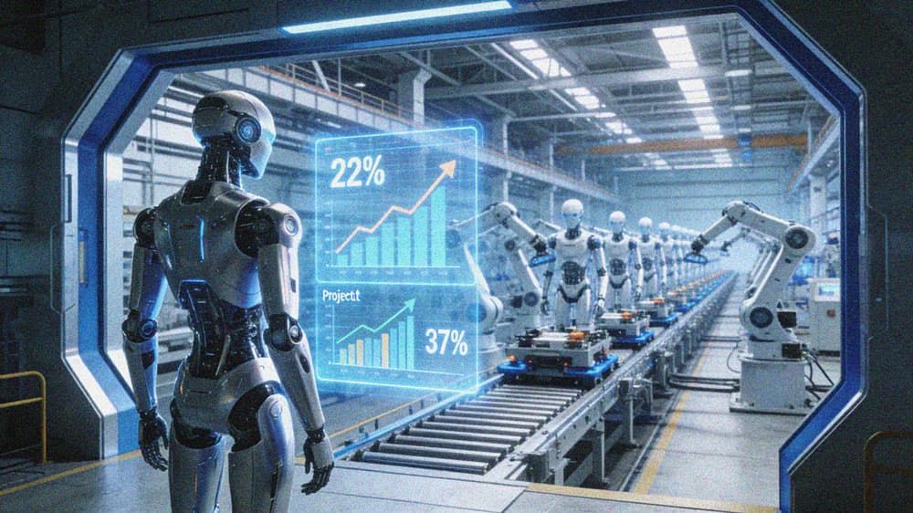
The core bottleneck for the commercial mass production of AI humanoid robots lies not only in core components such as motion control algorithms and servo motors, but also in the high-density PCBs (printed circuit boards) supporting the overall signal transmission and power supply. These PCBs need to be adapted to the miniaturized, highly reliable, and multi-condition adaptability characteristics of humanoid robots. The traditional "design-manufacturing" separation model can no longer meet mass production requirements. The Integrated Product Design & Manufacturing (IPDM) system, by connecting the entire chain of design, process, production, and testing, has become the core tool for solving the mass production challenges of humanoid robot PCB solutions.
IPDM: The Core Logic of High-Density PCB Mass Production for Humanoid Robots
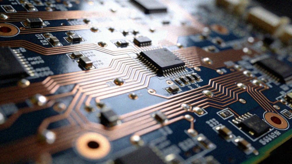
The PCBs for humanoid robots differ from those used in consumer electronics and industrial equipment. The PCBs for their joint modules, main control units, and sensing modules must simultaneously meet three core requirements: high-density wiring (line width and spacing ≤ 3mil/3mil), resistance to mechanical vibration (≥10g vibration acceleration), and wide operating temperature range (-20℃~70℃). Furthermore, there are over 20 different types of PCBs for the entire robot, and the small-batch, multi-batch production characteristics further increase manufacturing complexity.
The core value of IPDM lies in breaking down the information barriers between design and manufacturing, bringing "Manufacturability (DFM), DFP, and DFT" to the PCB design stage, and optimizing the design solution in reverse with mass production as the guiding principle. Compared to the inefficient traditional model of "design completed, then handed over to manufacturing, only to rework upon discovering problems," the IPDM system involves both design and manufacturing teams from the requirements definition stage. Based on the actual working conditions of the humanoid robot (such as joint bending angles and the heat dissipation power of the main control unit), customized Humanoid robot PCB solutions are developed, avoiding design redundancy and process incompatibility issues from the outset. This is crucial for ensuring high PCB mass production yield and controllable costs.
Design Stage: IPDM Drives Precise Optimization of High-Density PCBs
High-density PCB design is the first hurdle in the mass production of humanoid robot PCBs. Taking the 8-layer high-density PCB of the humanoid robot's main control unit as an example, it needs to integrate dozens of components such as the CPU, communication chips, and sensor interfaces, with over a thousand blind and buried vias. Signal integrity (SI) and power integrity (PI) directly affect the overall control accuracy of the robot.
Under the IPDM system, design-phase optimization focuses on three core dimensions:
Work Condition-Driven Pre-Simulation: Based on the actual motion conditions of the humanoid robot, vibration simulation, thermal simulation, and signal simulation are completed using professional tools such as Ansys and Mentor Graphics. For example, for the rigid-flexible PCB of the joint module, the design team needs to combine the joint bending angle (usually ≤120°) and bending times (≥100,000 times) to confirm the adhesive selection and copper foil thickness (1oz/2oz) of the rigid-flexible bonding area with the manufacturing team within the IPDM framework, avoiding delamination and breakage issues during mass production;
Deep Integration of DFM Rules: The manufacturing end transforms process capabilities such as laser drilling, micro-pitch welding, and AOI inspection into a design rule library and embeds it into the design software. For example, for line widths and spacings of 3mil/3mil, the manufacturing team pre-defined the process limit of "laser drilling hole diameter deviation ≤ ±0.01mm," allowing the design team to optimize the wiring layout accordingly and avoid short-circuit risks caused by mismatches between hole diameters and pads.
Material Standardization and Collaboration: The IPDM system links procurement, design, and manufacturing, establishing a qualified supplier list for special materials used in humanoid robot PCBs (such as high thermal conductivity copper-clad laminates and high-temperature resistant solder resist inks), preventing supply disruptions in mass production due to the selection of niche materials during the design phase. According to publicly available data from the PCB industry, this model can reduce material compatibility issues in the design phase by more than 70%.
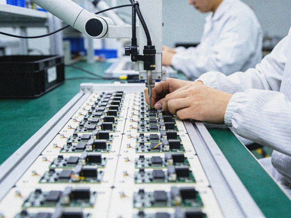
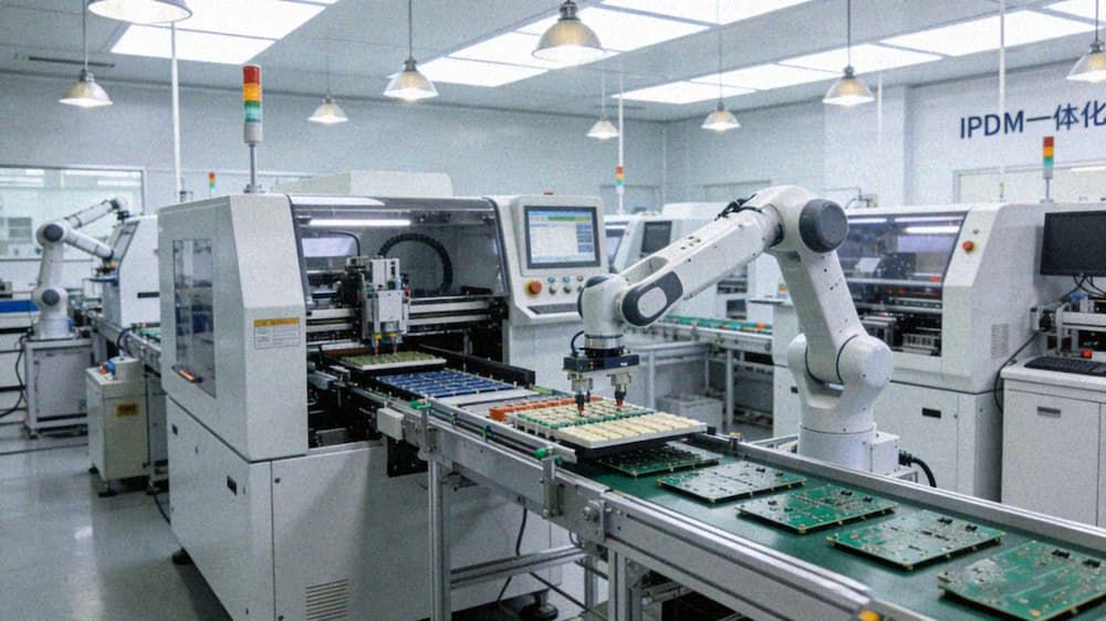
Manufacturing Phase: IPDM Achieves End-to-End Collaboration and Yield Improvement
The manufacturing process of high-density PCBs is far more complex than that of conventional PCBs. Core processes such as drilling, electroplating, and etching alone have more than 50 key parameters, and deviations in any of these steps can lead to a sharp drop in yield. IPDM achieves precise control over the entire manufacturing process through real-time linkage of "design parameters - process parameters - inspection standards."
In the drilling process, to address the blind and buried via requirements of humanoid robot PCBs, the IPDM system simultaneously outputs data such as hole position coordinates and hole diameter tolerances from the design end. The manufacturing end directly calls upon the parameter library of the laser drilling equipment, controlling drilling accuracy within ±0.005mm, reducing the scrap rate by 40% compared to traditional mechanical drilling. In the electroplating process, based on the current density requirements from the design end, the manufacturing end dynamically adjusts the electroplating time and current parameters to ensure uniform plating thickness (deviation ≤ ±0.5μm), meeting the stability requirements of signal transmission. In the inspection process, IPDM transforms key nodes from the design end (such as the power and signal layers of the main control PCB) into key areas for AOI inspection. Combined with X-ray inspection technology, it achieves accurate defect identification, improving inspection efficiency by 30%.
In a humanoid robot mass production project, a leading robotics enterprise adopted Kingbrother’s IPDM one-stop solution for core control system development and mass production. By applying car-level design, composite thermal management, modular hardware architecture, and DFM/DFA optimization, the enterprise achieved significant improvements:
- High-density PCB mass production yield increased from 75% to 88%
- Overall delivery cycle shortened from 25 days to 18 days
- Hardware development complexity reduced, product stability and environmental adaptability enhanced
This result is consistent with the mass production efficiency and quality improvement range of top domestic PCB manufacturers serving the humanoid robot industry.

Industry Value of IPDM in Enabling Mass Production of Humanoid Robot PCBs
The mass production of AI humanoid robots is essentially a transformation from "technical feasibility" to "commercial feasibility," with the cost and yield of high-density PCBs being the core variables. IPDM not only solves the mass production problem of individual PCBs but also, through end-to-end data accumulation, forms reusable Humanoid robot PCB solutions templates. For different humanoid robot models, only design parameters and process adaptation items need to be adjusted to quickly complete PCB design and mass production, significantly reducing R&D and manufacturing costs.
Simultaneously, the "design-manufacturing" collaborative model under the IPDM system is also driving PCB manufacturers to transform from "processors" to "solution providers," forming a deeply integrated cooperative relationship with humanoid robot companies. This is the core competitiveness of the PCB industry in entering the humanoid robot market.
Conclusion
The wave of mass production of AI humanoid robots is forcing upstream supply chain model innovation. High-density PCBs, as the "nerves and blood vessels" of the entire robot, require end-to-end optimization in design and manufacturing for mass production. By breaking down information barriers, implementing proactive risk management, and optimizing end-to-end collaboration, the IPDM system not only addresses the current mass production pain points of Humanoid robot PCB solutions but also constructs a closed loop of "demand-design-manufacturing-iteration," laying a core foundation for the commercialization of AI humanoid robots from the laboratory. In the future, with the deep integration of IPDM with digital simulation and intelligent manufacturing technologies, the yield and cost of high-density PCBs will be further optimized, becoming a key force driving the large-scale deployment of AI humanoid robots.