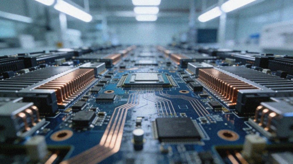
With the explosive growth of AI computing power, the hardware requirements for servers, edge computing devices, and various accelerator cards have reached unprecedented levels. As the physical foundation supporting all of this, the design and manufacturing of the PCB directly determines the upper limit of system performance. High-speed AI PCB design is no longer a simple circuit connection, but a complex systems engineering project involving signal integrity, power integrity, thermal management, and high-density interconnects. Simply focusing on signal paths or power networks is insufficient to meet the challenges; SI/PI collaborative optimization has become the key to design success or failure.
Core Challenges of High-Speed AI PCB Design
hardware, such as computing server motherboards, typically possesses several significant characteristics: extremely high computing density, massive data throughput, and complex power supply systems. This directly translates into stringent requirements for the PCB.
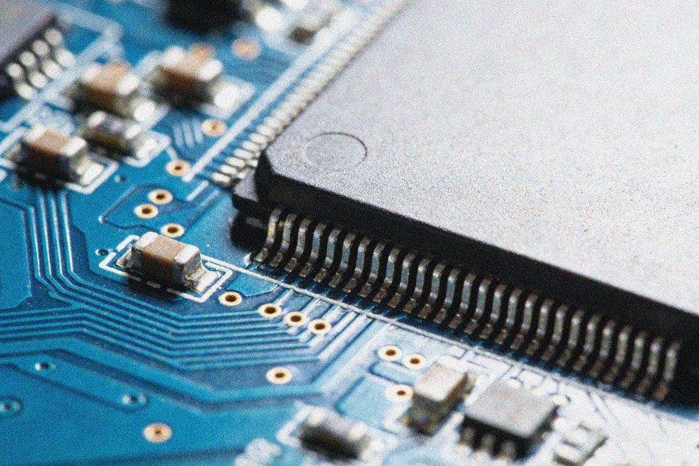
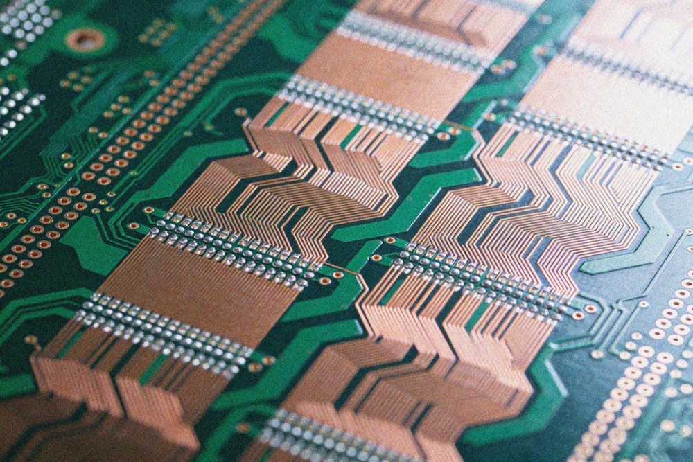
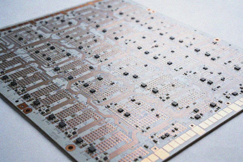
First, there is the high-density interconnect. Taking KINGBROTHER's high-multilayer AI computing server motherboards as an example, their layer count ranges from 16 to 32, aiming to maximize wiring space within a limited board area. Its CAM design requires linewidths and spacings of 4.5/2.5 mils, with a minimum distance of 7 mils from inner-layer vias. At this density, crosstalk control and impedance continuity become exceptionally difficult.
Secondly, there's the challenge of high-speed signal transmission. Data exchange rates between AI chips and between chips and memory often reach tens of Gbps. Technical data shows that in the prototype stage, the highest signal transmission rate on a PCB can reach 112 Gbps, while mass-produced boards can support 25 Gbps. This means that control over losses, reflections, and timing must be extremely precise. For example, in 400G high-speed optical module products, impedance tolerance needs to be controlled with in ±8%.
Finally, there are severe challenges in heat dissipation and power supply. High computing power means high power consumption; concentrated and enormous currents will generate significant IR voltage drops and noise on the power distribution network, while also generating a large amount of heat. Improper thermal design will not only trigger chip throttling but also degrade signal quality due to material parameters (such as Dk values) drifting with temperature, creating a vicious cycle of SI and PI issues and thermal management.
Impedance Control and Stacking Design – The Foundation for Collaborative Optimization
All high-speed designs begin with a well-thought-out stacking structure. The stack determines the integrity of the signal reference plane, the isolation between signals on different layers, and the distribution of power/ground planes, forming the common foundation for SI and PI.
In the evaluation board design for the NVIDIA Jetson AGX Xavier module, the team used a 10-layer, approximately 1.6mm thick board to meet the challenge of 750Gbps high-speed I/O. The core idea of this stack is to provide a complete, low-impedance return path for signals. Four layers are dedicated to ground planes, which not only provides a stable reference for high-speed signals, significantly reducing loop area and electromagnetic interference, but also lays the foundation for low impedance in the power system.
For differential signals, such as high-speed SerDes channels or DDR memory interfaces, their characteristic impedance is typically strictly controlled to 100 ohms (90 ohms for certain specific traces). This requires precise calculation of linewidth, line spacing, and distance to the reference plane based on the dielectric constant of the selected high-speed materials (such as TU933+ commonly used in AI server motherboards, or M6 and TU872SLK used in high-speed backplanes). In high-level boards, it is also necessary to model and match the propagation delay of inner and outer layer signals to ensure timing consistency.
Power Integrity Optimization – Providing “Clean Energy” for Computing Power
An unstable power supply will directly inject noise into the signal channel, leading to eye diagram closure and increased bit error rate. Therefore, the goal of PI design is to ensure that the voltage ripple reaching the chip power pins is within acceptable limits under any load transients.
In the case of the Jetson evaluation board, in addition to multiple ground planes, the power plane is deliberately placed close to the ground plane to form efficient planar capacitors and reduce the impedance of the power network. Furthermore, a real-time monitoring and management module is onboard to dynamically balance the power supply and actively suppress power noise. This design approach is even more critical in large AI server motherboards, where the CPU, GPU, and memory power consumption can reach hundreds of watts, with drastic instantaneous current fluctuations.
Power electronics industry solutions also confirm this. For example, in high-power applications such as converter valve control boards, designs employ independent power layer layouts and use thickened copper foil (e.g., 3-6OZ) to carry high currents, reducing line impedance and temperature rise. For AI motherboards, while the current may not be as extreme, planning a dedicated, low-impedance power layer for the core voltage (e.g., VDD_CORE) in multi-layer PCBs, supplemented by a large, evenly distributed network of decoupling capacitors, is standard practice to ensure PI performance.
Co-design of Thermal Management and Signal Integrity
Heat is a hidden killer of signal integrity. High temperatures can cause changes in the dielectric constant of the PCB substrate, affecting impedance stability and exacerbating transmission line losses. Therefore, thermal management must be incorporated into the co-design framework of SI/PI.
In the design of high-power modules like the Jetson AGX Xavier, thermal management solutions are considered upfront. The evaluation board supports multiple power consumption levels of 10W/15W/30W and has a wide operating temperature range of -25°C to 80°C. The PCB design team needs to collaborate closely with structural engineers, focusing on the thermal design of the controller to ensure its reliability under high loads. This may involve designing thermal pads, thermal via arrays, or even pre-embedded copper blocks or using high thermal conductivity materials on the bottom of the PCB or under critical chips to efficiently dissipate heat.
This collaboration is also reflected in other products, such as thermally separated copper substrates and locally embedded ceramic PCBs. While these are extreme solutions for specific high-power scenarios, their core concept—considering heat flow paths during the placement and routing phase to avoid over-concentration of heat-sensitive and high-power components and prevent local hotspots from affecting overall performance—is equally applicable to high-speed AI PCB design.
Simulation-Driven Design and DFM Closed Loop
Before entering the expensive prototyping and testing phase, using simulation tools for SI/PI collaborative analysis and optimization is the only way to reduce costs and shorten the cycle time. KINGBROTHER, through long-term practical experience, has independently developed the KBEDA SKILL tool based on the Cadence platform. This tool integrates over 400 application functions specifically for signal integrity analysis in high-speed PCB design.
This tool can simulate and predict signal reflection, crosstalk, and delay issues during the design phase, allowing engineers to perform more precise optimizations. For example, in power integrity, it can perform IR-Drop voltage drop analysis and PDN impedance analysis to identify power supply bottlenecks early; in signal integrity, it can perform timing simulations for DDR4/5 parallel signals and optimize simulations for high-speed serial channels (e.g., 25Gbps to 112Gbps).
However, simulation must be closely integrated with design for manufacturability. A perfect simulation model is meaningless if it cannot be achieved through manufacturing processes. In mass production, the company can achieve a minimum line width and spacing of 2.5/2.5 mil (FR4) and a minimum mechanical drill hole diameter of 0.2mm. These process boundaries are the constraints of the simulation design. For example, in the case of high-layer HDI boards in microelectronic bonding equipment, the precise positioning requirements of HDI stacked vias on 22-layer boards were solved by using "multi-stage laser processing technology for via alignment" and "high-multilayer alignment lamination technology," ensuring that the high-density interconnect scheme designed in simulation could be reliably implemented in actual production.
AI-driven high-speed PCB design is a multi-dimensional art of balance. Signal integrity, power integrity, and thermal management are no longer isolated design silos, but rather a unified whole that must be planned and optimized collaboratively from the very beginning of the project. From precise stacking and impedance control based on high-speed materials (such as TU933+), to building low-impedance power networks for multilayer, high-current boards, and to thermal design and simulation verification throughout the entire process, every decision is interconnected.
Successful AI signal integrity PCB design ultimately manifests as a series of quantifiable and manufacturable parameters: achieving fine 4.5/2.5 mil traces on 16-32 layer boards, impedance tolerance within ±8%, channel performance meeting 112Gbps transmission rates, and heat dissipation and power supply capabilities ensuring long-term stable operation of the system in harsh environments. This is precisely the engineering practice of reliably translating the chip's powerful computing capabilities into actual product performance through deep SI/PI co-optimization.