The necessity of cost reduction in the context of the AI edge device mass production boom
As AI edge devices enter mass production, many teams discover that performance targets are achievable—but cost, yield, and cycle time quickly become the real bottlenecks.
Issues such as the lengthy PCB prototyping cycle, high trial-and-error costs, insufficient compatibility between advanced packaging technology and mass production demands, low yield rates, and ineffective cost waste caused by disconnection between design and manufacturing have become the core pain points restricting the enterprises' profitability. This article focuses on the two core aspects of PCB prototyping and advanced packaging, integrating practical technologies, real data, and implementation cases, to dissect the directly reusable cost reduction innovation solutions, helping enterprises achieve a two-way breakthrough in cost control and efficiency improvement during large-scale production.
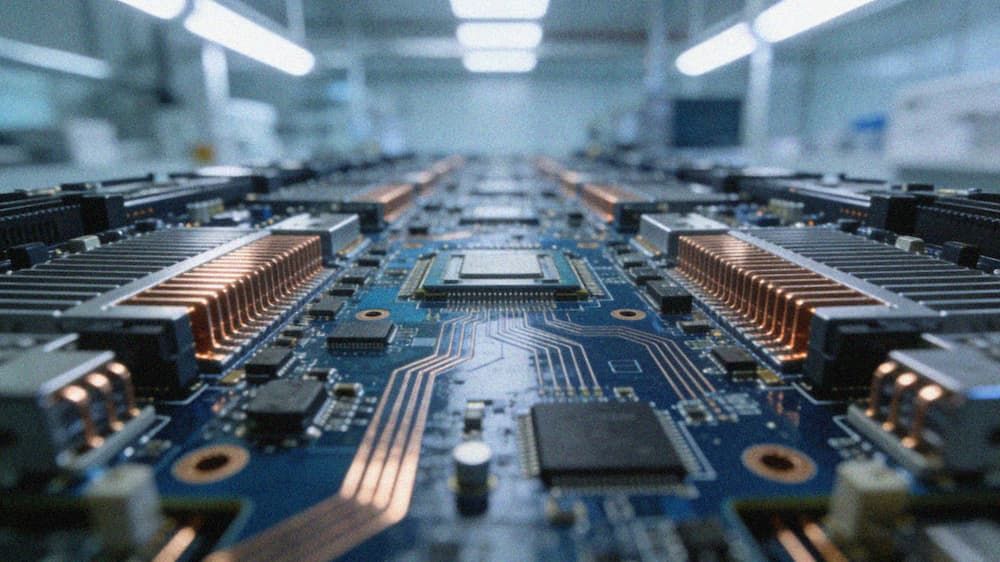
AI Hardware PCB Prototype Cost Reduction Innovation: Full-Dimensional Optimization from Design to Process
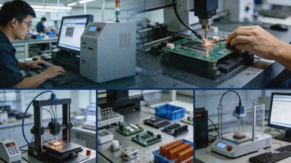
Based on multiple AI edge device mass production projects delivered by KINGBROTHER, PCB prototype testing is a crucial verification step before the mass production of AI hardware, and its cost and cycle control directly determine the overall production efficiency. Through a full-chain adjustment of material selection optimization, process technology innovation, and design pre-control, it is possible to achieve precise cost reduction during the prototype stage while ensuring the stability of product performance.
In terms of material selection, replacing high-cost materials with cost-effective ones and achieving domestication compatibility have become the core path for cost reduction. We have abandoned the traditional model of relying on imported materials and instead selected the domestic Shengyi S1000H material. This not only meets the core requirements of AI edge devices for high-temperature stability (170℃+) but also reduces the material cost by 18%-25%. The surface treatment process adopts domestic gold plating and tin plating solutions. While ensuring the reliability of welding, corrosion resistance, and stable signal transmission, it further reduces the premium costs brought by imported processes, meeting the cost expectations for large-scale mass production.
Process innovation provides the core impetus for improving the efficiency and cost optimization of prototyping.
The application of HDI multi-layer interconnection technology and integrated prototyping process for rigid-flex boards, combined with the rapid-turn prototype manufacturing service, breaks the constraints of traditional prototyping cycles, compressing the original 7-10-day prototyping cycle to 24-48 hours, and directly reducing the cost of small-batch prototyping by 30%. At the same time, the high-density SMT process and integrated anti-corrosion coating treatment are implemented simultaneously, adapting to the mass production process standards in advance, and reducing the repetitive costs caused by subsequent process adjustments.
Pre-design optimization can avoid the cost of trial and error at the source, and is a key approach to reducing the cost of prototyping. Relying on a 3.27 million-certified material library and a 2,368-item DFM (Design for Manufacturing) rule library, through DFM simulation for manufacturing and SI/PI signal simulation before prototyping, it can accurately predict potential process conflicts and signal interference issues that may occur during mass production, thereby pre-emptively avoiding 80% of the risks in mass production. The deep application of modular reusable design has enabled the PCB design reuse rate to reach 68%, far exceeding the industry average of 35%, significantly reducing the time and cost losses caused by repeated design and repeated prototyping.
Comparison of Core Indicators between Traditional PCB Prototype Production and Innovative Prototype Production
| Comparison Dimension | Traditional Proofing | Innovative Proofing (KINGBROTHER Solution) | Cost Reduction/Efficiency Enhancement Margin |
|---|
| Sample production cycle | 7-10 days | 24-48 hours (rapid sample production) | Cycle is compressed by over 70% |
| Material cost | Imported base material accounts for more than 60% | Domestic compatible base material accounts for more than 90% | Material cost reduced by 18%-25% |
| Number of trial-and-error attempts | 3-5 times | 1-2 times (DFM pre-optimization) | Trial-and-error cost reduced by more than 60% |
| Mass production yield | 85%-90% | 98.5% (EMC pass rate) EMC compliance based on IEC / IPC standards | Yield increased by 8.5-13.5 percentage points |
Description: The design adopts a left-right column comparison layout. On the left side, a traditional proofing "design → proofing → testing → rework → re-proofing" closed-loop consumption model is presented, with the time consumption ratio of each stage marked. On the right side, an innovative proofing "DFM design optimization → modular reuse → rapid proofing → one-time success" linearly efficient path is displayed. The core optimization actions (domestic substrate substitution, SI/PI simulation verification, integrated process integration) are highlighted in the middle. At the bottom, the overall cost reduction and efficiency improvement data are marked, presenting the optimization logic and actual value intuitively.
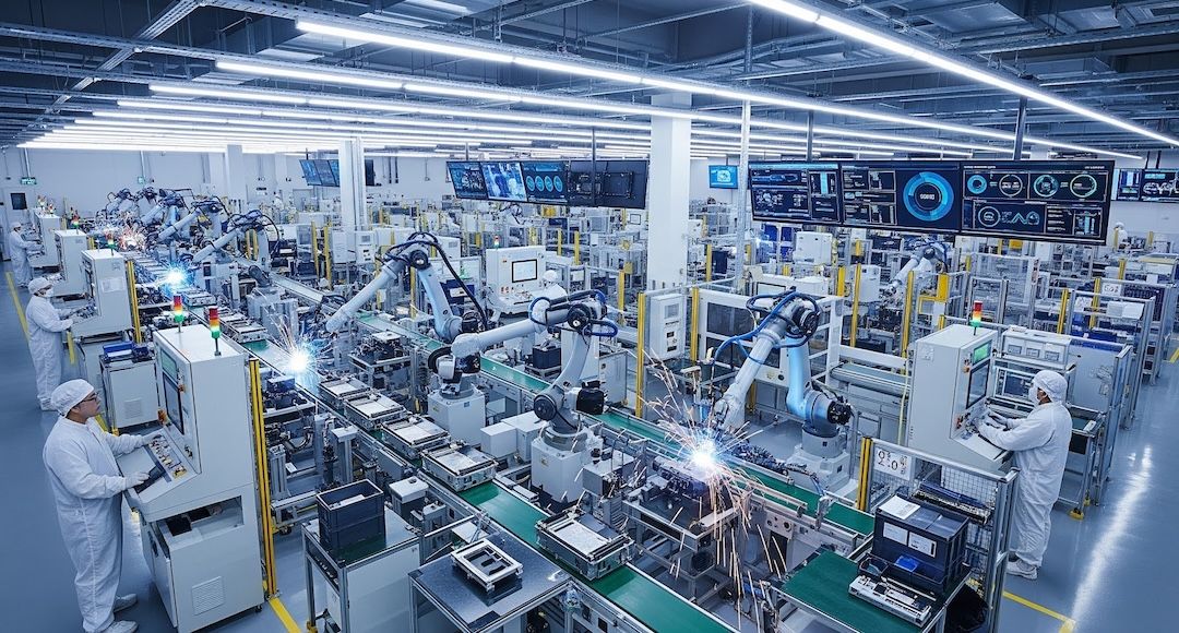
AI Hardware Advanced Packaging Cost Reduction Solution: Miniaturization, Integration and Process Innovation
Advanced packaging is the core support for the miniaturization, high integration and high performance of AI edge devices. The cost control in this field needs to take into account both technical compatibility and the requirements of large-scale mass production. Through precise technology selection, process innovation and supply chain collaboration, a balance and optimization of cost and yield can be achieved.
In terms of technology selection, we focused on the core requirements of lightweight and miniaturization for AI edge devices, and prioritized the use of SIP (System In Package) system-level packaging, three-dimensional assembly packaging, and rigid-flexible integration packaging solutions. This not only reduced the product size but also decreased the number of components and assembly steps. The core component packaging adopted domestic alternative solutions, replacing imported similar products with MagnTek-MT6835GT driver chip packaging. Without adjusting the overall circuit design and assembly process, a 22% reduction in packaging costs was achieved, while maintaining the same performance parameters as the imported products and fully meeting the requirements for mass production.
Process innovation has become the core breakthrough point for reducing costs in large-scale packaging.
The combined application of high-density SMT technology, integrated anti-corrosion coating treatment, and nitrogen-hydrogen reflow soldering process (strictly following IPC-A-610G III standards) effectively improves packaging accuracy and reliability, increasing the traditional packaging yield from 92% to 97%, and reducing the batch packaging cost by 15%-20%. To meet the complex working conditions of AI edge devices, additional precision control of metallization slot holes and multiple back-drilling techniques are added, further strengthening the anti-interference and stability of the packaging, and reducing the costs of later maintenance and rework.
Supply chain collaboration provides a guarantee and support for reducing costs in packaging. Relying on the KBOM technology platform, we achieve intelligent matching and rapid switching of multiple alternative materials, reducing the replacement cycle of old components by 40% and avoiding production halts due to material shortages. Through centralized procurement of domestic components and bulk bargaining, we further compress supply chain costs. At the same time, we establish a long-term cooperation mechanism with core suppliers to ensure the stability and consistency of material supply and quality, and avoid cost risks caused by price fluctuations.
Comparison of Costs and Yield Rates of Different Packaging Schemes
| Packaging Solution | Applicable Scenarios | Cost Level (Yuan/Unit) | Mass Production Yield | Core Logic of Cost Reduction |
|---|
| Traditional discrete packaging | Early prototypes, low-integration devices | 80-120 | 90%-92% | No obvious cost reduction potential, only suitable for small-scale trial production |
| SIP integrated packaging | Smart terminals, sensor modules, lightweight equipment | 50-75 | 95%-96% | Device integration reduces assembly steps, reduces volume and lowers auxiliary material costs |
| Three-dimensional assembly packaging | Robot-driven boards, power modules, high-power equipment | 60-85 | 96%-97% | Space optimization improves integration, process reuse reduces debugging costs |
| Domestic substitution packaging | Full-scenario mass production compatibility, cost-sensitive equipment | 45-65 | 94%-96% | Domesticated components have lower premium prices, further cost reduction through batch purchasing |
Description: The sectional visualization design is adopted to clearly display the three-dimensional stacked integration structure of the chip, sensor, and passive components, and mark the core cost reduction design details (domestic MagnTek-MT6835GT driver chip, integrated three-proof coating layer, high-density interconnection lines); on the right side, an additional size comparison chart is provided, marking the volume difference between the traditional discrete packaging and SIP integrated packaging (reduced by 40%); below, core data such as packaging yield and cost reduction are supplemented, visually demonstrating the dual advantages of miniaturization and cost reduction.
Full-process collaborative cost reduction: The core value of the IPDM one-stop solution
The optimization of cost reduction in a single process is difficult to achieve the maximum overall production efficiency. The IPDM (Integrated Product Design and Manufacturing) solution, by integrating the entire design, manufacturing, and supply chain processes, breaks down the information barriers between different links and realizes the full-process cost control from R&D to production, thereby enhancing the overall cost reduction efficiency and stability.
The design-manufacturing loop is the core logic for achieving overall cost reduction throughout the entire process. By integrating IPD (Integrated Product Design), IPM (Integrated Product Manufacturing), and the PCB business, the manufacturing requirements are brought into the design process in advance, avoiding the situation where the design plan and the production process are disconnected, resulting in rework costs. Leveraging the 56-layer 112Gbps high-speed PCB design capability and 68% modular reuse rate, the success rate of the solution is significantly improved, and the production cycle is compressed to 60% of the industry average, effectively reducing the time and cost losses caused by design adjustments.
The full life cycle optimization of BOM runs throughout the entire production process, achieving dynamic cost control. The 3.27 million certified material library and the domestic substitution solution library provide support for BOM optimization. Through precise selection, the procurement cost of common components can be reduced by 15% - 20%. The full life cycle BOM risk warning mechanism can predict risks such as chip shortage, price fluctuations, and component obsolescence in advance, reducing the risk of shortage by 80% and shortening the replacement cycle of old components by 40%, ensuring the continuity of production.
The flexible adaptation capability of the supply chain ensures the realization of scale effects. From multi-source material matching, batch inventory planning, to 24-hour closed-loop response to production issues, the IPDM solution enables a smooth transition from small-batch trial production to large-scale mass production, avoiding production halts and cost increases due to capacity fluctuations and material shortages; at the same time, it collaborates with core suppliers to establish a coordination mechanism, achieving material price locking and quality control synchronization, further enhancing the advantages of large-scale cost reduction.
Description: The architecture is designed in a hierarchical manner. The top layer is the demand layer, clearly stating the core demands for reducing production costs of AI edge devices (cost reduction, shortened cycle, and improved yield); the middle layer is the collaborative core layer, horizontally connecting four major processes: "IPD design optimization → IPM manufacturing cost reduction → PCB process innovation → KBOM supply chain optimization". Each process is marked with key actions and corresponding cost reduction data (design optimization reduces costs by 15%, manufacturing cycle is compressed by 30%); the bottom layer is the result output layer, summarizing and presenting the core achievements of a 15%-25% overall cost reduction, a 30%-40% shortened production cycle, and a product yield of ≥ 97%, clearly demonstrating the logic of full-chain collaborative cost reduction.
Practical Case: Verification of Cost Reduction for AI Edge Devices in Mass Production
Case 1: Main Control System for Intelligent Lawn Mowers
In the cost reduction process of the main control system for intelligent lawn mowers, the main challenges were concentrated on the frequent trial and error in PCB prototyping due to the high precision requirements of sensors, as well as the insufficient heat dissipation performance of the packaging affecting the stability of the equipment. To address these issues, the Horizon Sunrise X3 processor was adopted as the core chip, combined with high thermal conductivity aluminum-based thick copper materials for PCB prototyping, and a three-dimensional assembly packaging solution was used to equip the main board with an efficient heat dissipation plate to optimize the heat dissipation effect. By integrating DFM pre-optimization and modular design, the number of prototyping trial and error was reduced from 3 times to 1 time, the prototyping cost was decreased by 28%, the mass production yield was stable at 98%, and the problems of heat dissipation and precision compatibility were completely solved, meeting the usage requirements in complex outdoor conditions.
Case 2: Infrared Camera Control System
The infrared camera control system is widely applied in the intelligent scenarios of elderly care and medical devices. However, it faces the challenges of insufficient real-time performance of sensor data fusion, low packaging reliability in electromagnetic interference environments, and high production costs for batch production. The solution adopts the RV1126K high-performance AI visual processing chip, using SIP integrated packaging and EMC optimized design, combined with high-density SMT process and nitrogen reflow soldering packaging technology, to enhance the system's anti-interference ability and data processing efficiency. Ultimately, the packaging cost is reduced by 22%, the anti-interference ability is improved by 35%, the production cycle is shortened by 30%, and it is fully compatible with complex usage environments such as strong light and electromagnetic interference.
Case 3: AI Computing Power Server Motherboard
The AI computing power server motherboard, as the core component of high computing power edge devices, has extremely high requirements for PCB high-density interconnection and signal stability. The traditional solution has problems such as severe electromagnetic interference, long prototyping cycle, and low yield. By selecting TU933+ high-speed substrate and adopting a 16-32 layer PCB prototyping design, the line width and line spacing are precisely controlled at 4.5/2.5 mil. Combined with HDI technology and layout and wiring optimization, the signal transmission stability is improved. After optimization, the prototyping cycle is reduced from 10 days to 3 days, the prototyping cost is decreased by 19%, the production yield is stable at over 97%, the signal transmission stability is increased by 35%, and it meets the requirements of high computing power scenarios.
Implementation Suggestions for Mass Production Cost Reduction: The Path from Pilot Production to Large-scale Deployment
For mass production cost reduction, a step-by-step implementation approach should be adopted, with phased optimization plans to ensure the balance between cost control and product quality.
Preparatory Stage (1-2 weeks)
Precisely analyze the equipment operation requirements, clearly define core indicators such as temperature, humidity, anti-interference, and heat dissipation. Based on this, select PCB materials and packaging solutions. At the same time, conduct pre-simulation verification using DFM tools to optimize the design and BOM list, determine the proportion of domestic alternative components, and reach an initial cooperation intention with core suppliers to avoid risks in the initial selection process.
Pilot Production Verification Phase (2-4 weeks)
Carry out a small batch production verification plan of 50-100 pieces to verify the feasibility of the scheme. Collect key data such as PCB sample pass rate, packaging reliability, heat dissipation performance, and signal stability. Optimize process parameters and BOM list specifically to solve compatibility issues encountered during pilot production and determine the final mass production plan. At the same time, negotiate material prices and supply cycles with suppliers, establish quality control standards, and make preparations for large-scale mass production.
Large-scale Production Stage
Focus on stability and continuous optimization. Sign a batch purchase agreement with suppliers to lock in material prices and avoid the risk of price fluctuations; activate a 24-hour production issue response mechanism to quickly solve process and material problems in production, ensuring stable yield; regularly review BOM costs and process efficiency data, combined with technological iterations and changes in the supply chain, continuously optimize cost reduction plans to expand the cost advantage of large-scale production.
Future Trends of Cost Reduction in Mass Production of AI Edge Devices
The future development of cost reduction in the mass production of AI edge devices will be deeply driven by the dual forces of technological iteration and ecological collaboration. Technologically, AI-assisted PCB design tools will further enhance design efficiency and accuracy, while miniaturization and high-integration packaging technologies will continue to make breakthroughs, driving continuous cost reduction; Supply chain-wise, the maturity of domestic components and substrates will continue to improve, breaking the reliance on imports, and the integrated services of design, manufacturing, and supply chain will become the mainstream in the industry, further compressing the costs of intermediate links.
It is worth noting that true mass production cost reduction does not merely involve cutting down material costs. Instead, it involves enhancing production efficiency through technological innovation, reducing ineffective losses through full-process collaboration, and achieving scale effects through ecological co-construction. For companies entering AI edge device mass production, choosing partners who can integrate design, manufacturing, and supply chain execution is becoming a decisive factor.