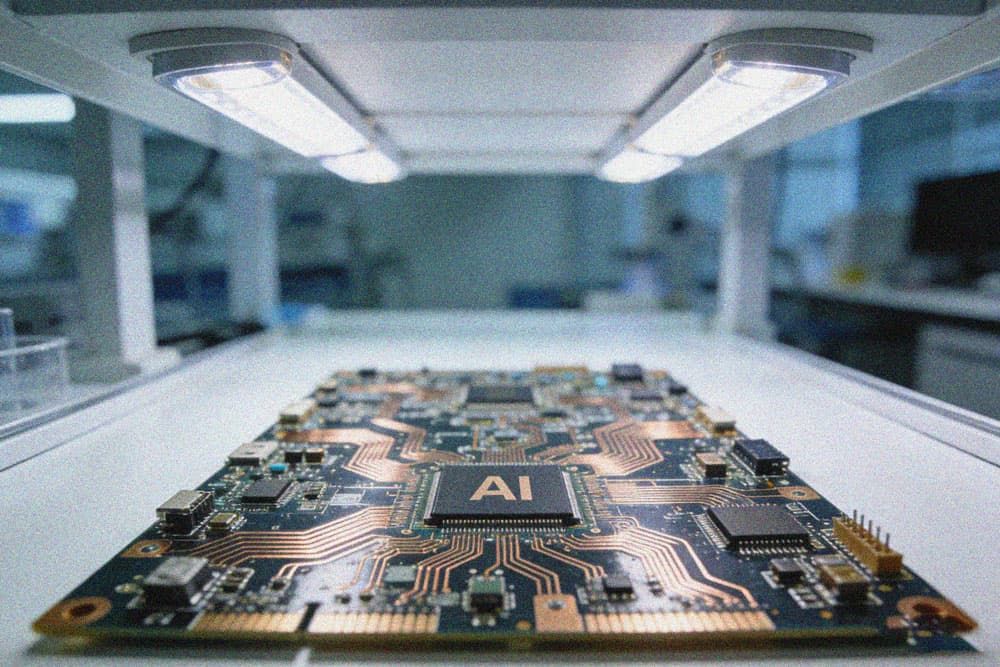
Embodied AI is bringing artificial intelligence from cloud algorithms into the physical world. Robots, intelligent vehicles, and autonomous devices—the "brains" of these systems—need to process massive amounts of sensory data and make real-time decisions, placing unprecedented demands on the hardware that supports them. As the core of electronic interconnect technology, the performance of the PCB (Printed Circuit Board) directly determines the computing density, reliability, and final form factor of this AI hardware.
At KINGBROTHER, we are providing the crucial physical foundation for this hardware breakthrough through a series of high-density, high-reliability PCB solutions. Our capabilities are not just talk; they are built on verifiable process parameters and successful cross-industry deliveries.
The Core Technology of High-Density Interconnect: From Parameters to Practice
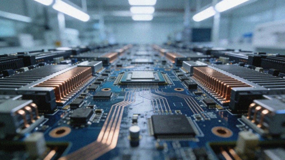
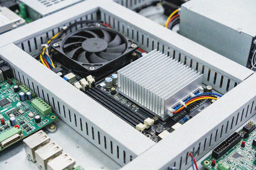
AI hardware, especially computing servers and edge controllers, faces the primary challenge of high-density interconnect design. This means integrating more computing units, memory chips, and high-speed interfaces within a limited board area, while ensuring stable signal transmission at tens of Gbps rates.
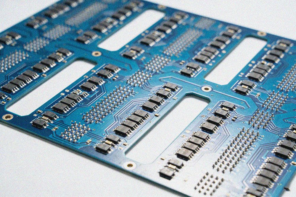
We have mature process technology for AI computing server motherboards. For example, our high-multilayer products utilize high-speed materials like TU933+, allowing for flexible configuration of 16 to 32 layers to meet varying power and signal routing complexity. To achieve high-density routing, inner layer trace width and spacing can be 4.5/2.5 mil (CAM design value), and the distance from inner layer holes to traces can be controlled to ≥7 mil after a single lamination. The overall board size can reach 450mm x 380mm, providing space for large motherboard layouts.
 High density also means extremely high precision requirements. We have mastered a minimum mechanical drilling hole diameter of 0.2mm (mass production standard, prototyping can reach 0.15mm or even 0.10mm), which is crucial for boards densely packed with high-pin-count BGA chips. Further capabilities are reflected in the control of special processes: precision control technology for metallized slots and crimp holes ensures reliable contact for high-power connectors; multiple back-drilling and high-density resin filling technology effectively eliminate stub-and-line effects in high-speed signal transmission, improving signal integrity.
These specific process parameters collectively constitute a hardware platform capable of supporting high-performance, high-bandwidth applications. It's not just a theoretical specification; it's the real foundation upon which we reliably deliver AI accelerator boards and server motherboards to numerous leading global companies.
Design Simulation and Manufacturing Closed Loop: Solving the Design Challenges of AI Embedded Systems
Manufacturing capabilities alone are insufficient. AI embedded system PCB design is a complete chain, from chip selection and circuit design to manufacturability implementation. The real challenge customers face is often: can the designed high-performance boards be manufactured efficiently and reliably?
This is precisely where the value of KINGBROTHER's IPDM (Integrated Product Design and Manufacturing) one-stop solution lies. We deeply integrate IPD (Integrated Product Design), IPM (Integrated Product Manufacturing), and the PCB platform, forming a closed loop between design and manufacturing.
On the IPD design side, our technology platform primarily utilizes ARM, FPGA, and GPU chip platforms. This means that from the solution design and hardware schematic design stages, we fully consider the power supply, heat dissipation, and signal layout requirements of these mainstream AI computing chips. Our EDA team performs high-speed PCB design and utilizes signal integrity (SI) and power integrity (PI) simulation tools for early verification. For example, in the evaluation board design based on the NVIDIA Jetson AGX Xavier module, we ensured stable performance of its 750 Gbps high-speed I/O through a 10-layer board stack-up, precise 100Ω differential impedance control, and a dedicated power management module design.
After design completion, collaboration between IPM and PCB manufacturing is crucial. Our IPM platform encompasses technologies such as KBOM (Materials Requirements Manufacturing), PCBA (Electronic Assembly Board), and EES (Engineering and Technical Services). Before mass production, the EES team conducts rigorous DFM (Design for Manufacturability) analysis, reviewing design documents using a rule base of over 2300 rules to proactively identify and resolve potential issues such as layout interference, pad mismatch, and poor heat dissipation paths. This "design-as-manufacturing" approach significantly reduces the anomaly rate during mass production.
In the PCB manufacturing phase, our capabilities cover the entire process from prototyping to mass production. For multilayer boards made of FR4 material, prototyping can achieve up to 68 layers, with mass production supporting 32 layers. Rigid-flex boards can be prototyped with a total of 30 layers (26 flexible layers), with mass production supporting 20 layers (12 flexible layers). These capabilities ensure a seamless transition from complex proof-of-concept boards to mass-produced boards.
AIoT & Robot Components Manufacturing involves the collaboration of numerous heterogeneous hardware modules. From sensing and computing to execution, each module has unique PCB requirements and must meet stringent standards for reliability, lightweight design, and environmental adaptability.
Our product portfolio covers key links in this chain. At the computing and control layer, we provide intelligent main control boards, robot main control boards, high-performance computing cards, and GPU/FPGA-based solutions. At the functional module layer, we offer head/chest control boards, communication boards, motor drive boards, etc. These products are not standard products but customized solutions based on specific customer scenarios.
For example, in humanoid robot projects, the main control board we provide uses the STM32H7 as the core processor. The design not only considers its multi-power domain architecture for low power consumption but also addresses the thermal management challenges of high computing power through automotive-grade design and a composite cooling system (such as integrated high-efficiency heatsinks). On the joint drive board, we use dedicated motor drive chips (such as the MagNTek-MT6835GT) and ensure stable output of the current required to drive high-power motors through thick copper PCB design and high-reliability soldering processes.
For more extreme integration needs, such as space-constrained and bending applications, our rigid-flex board solution has proven effective. In a surgical robot case, we replaced connectors with rigid-flex boards, achieving a highly reliable connection between two boards within a compact space. Our engineering team provided specific design guidelines: the distance from the via to the rigid-flex joint should be greater than 1mm, and the distance from the insertion hole to the joint should be greater than 1.5mm, ensuring long-term reliability under repeated bending.
Cross-Industry Validation: Reliability Stems from Specific Scenario Testing
The value of our solutions has been validated in complex projects across multiple industries. These cases don't rely on vague "industry reports," but rather on specific technical actions and quantifiable results.
In the automotive electronics field, a motor drive board needs to handle a peak current of 100A. The customer's initial solution posed a risk of copper foil overheating and burning. Our solution employed a 6oz thick copper design to enhance current carrying capacity, selected a high-Tg material (Tg≥170℃) to improve temperature resistance, and used high-thermal-conductivity PP sheets to optimize interlayer thermal conductivity. The final board met the overall system's heat dissipation requirements, reducing the customer's assembly and debugging cycle.
In the industrial control field, a bonding control board for a microelectronic bonding device requires a 22-layer high-multilayer HDI, with inner layer linewidth and spacing ≤2mil. The technical challenge lies in the high-multilayer alignment and the precision of HDI via stacking. We solved this problem through multi-layer laser processing technology for via stacking alignment and high-multilayer alignment lamination technology, significantly improving the product's soldering pass rate and saving substantial rework and repair costs.
In the medical device field, in addition to the rigid-flex PCB for surgical robots mentioned above, our pursuit of reliability permeates the entire process. Our manufacturing system is ISO13485 certified for medical device quality management systems. Our IPM process boasts capabilities for 01005 ultra-small component placement, 3D AOI inspection, full-process barcode tracking (meeting UDI requirements), and rigorous environmental and electrical safety testing, ensuring stable product operation in life-threatening scenarios.
The hardware breakthrough of embodied AI is an engineering race on the millimeter and micrometer scale. It requires not vague trend interpretations, but a deep understanding and precise control of material properties, transmission losses, thermal resistance, and process limits.
KINGBROTHER provides solid support for this race through verifiable high-density PCB process parameters, a closed-loop technology system from design to manufacturing, and concrete case studies in AIoT and robotics component manufacturing. We believe that reliable hardware is the prerequisite for intelligence to be "embodied."
If you are developing next-generation AI hardware and facing challenges in high-density interconnects, high-speed signal integrity, or high-reliability manufacturing, our solutions may offer a clear path.