As AI GPUs exceed 1TB/s memory bandwidth and 700W power consumption, conventional PCB architectures can no longer support signal integrity, power delivery, and thermal dissipation requirements. Advanced packaging substrates have therefore become a critical extension of chip performance.
To overcome the "memory wall" and "power wall," advanced technologies such as FC-BGA (Flip Chip Ball Grid Array) and 2.5D/3D packaging are becoming standard features of high-performance AI chips. The core carrier of this packaging revolution is the high-density interconnect (HDI) PCB and its advanced form—the packaging substrate. They are no longer merely "sockets" to hold chips, but have evolved into key subsystems determining system bandwidth, power consumption, and reliability.
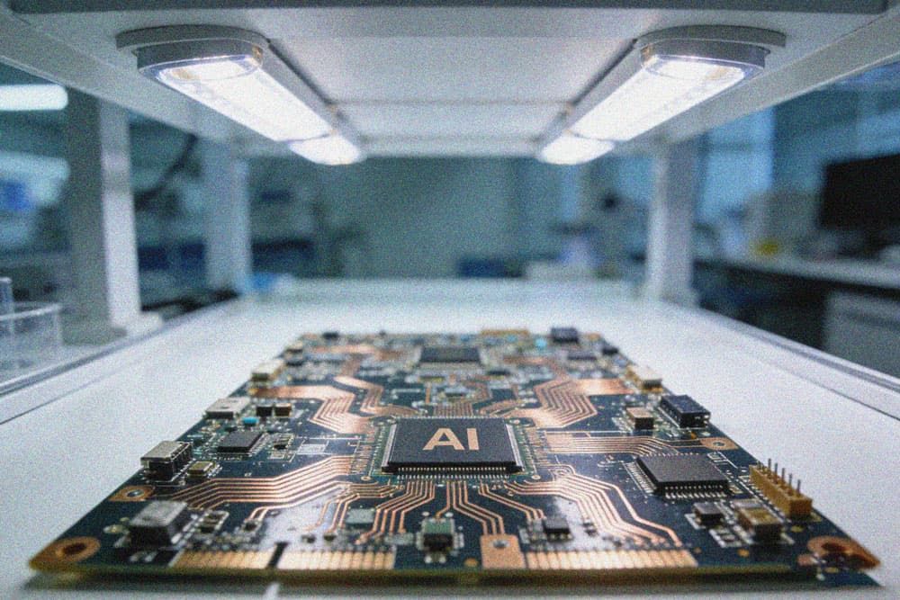
What Is an AI Chip Packaging Substrate?
An AI packaging substrate is a high-density interconnect carrier that electrically and mechanically connects AI processors, HBM memory, and system PCBs, enabling ultra-high bandwidth and power delivery beyond conventional HDI PCBs.
How AI Computing Power Demands Reshape PCBs and Substrates
Traditional server motherboard designs are struggling to handle the massive parallel processing and high-speed exchange of AI computing. This has directly spurred a new generation of AI computing PCB design concepts. The specific technical responses can be seen in KINGBROTHER's "AI computing power server motherboard high-multilayer products" from the knowledge base: the board material uses high-speed materials like TU933+, the number of layers is as high as 16-32, the minimum hole diameter is reduced to 0.2mm, and the line width and spacing reach 4.5/2.5 mil. These parameters are all designed to meet the requirements of high-bandwidth, low-latency signal transmission. However, when chips integrate more cores and HBM (High Bandwidth Memory) through advanced packaging, the requirements for the underlying substrate become even more stringent. This is the battleground for AI PCB advanced packaging. The packaging substrate needs to achieve tens of thousands of ultra-high-speed interconnects between the chip and memory, and between the chip and the motherboard, within an extremely small area. Its wiring density and signal integrity requirements far exceed those of conventional PCBs.
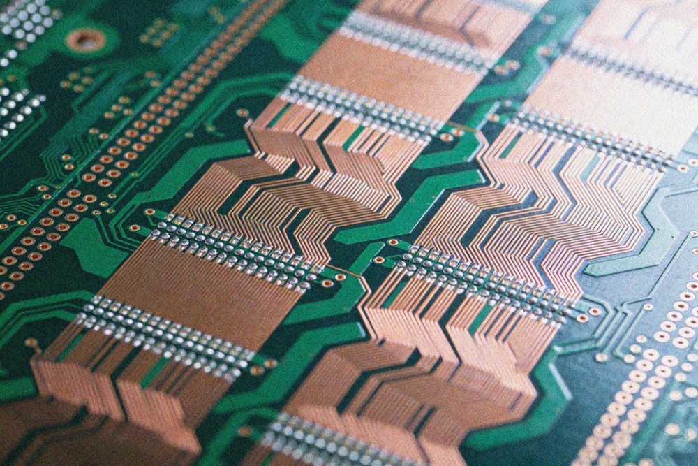
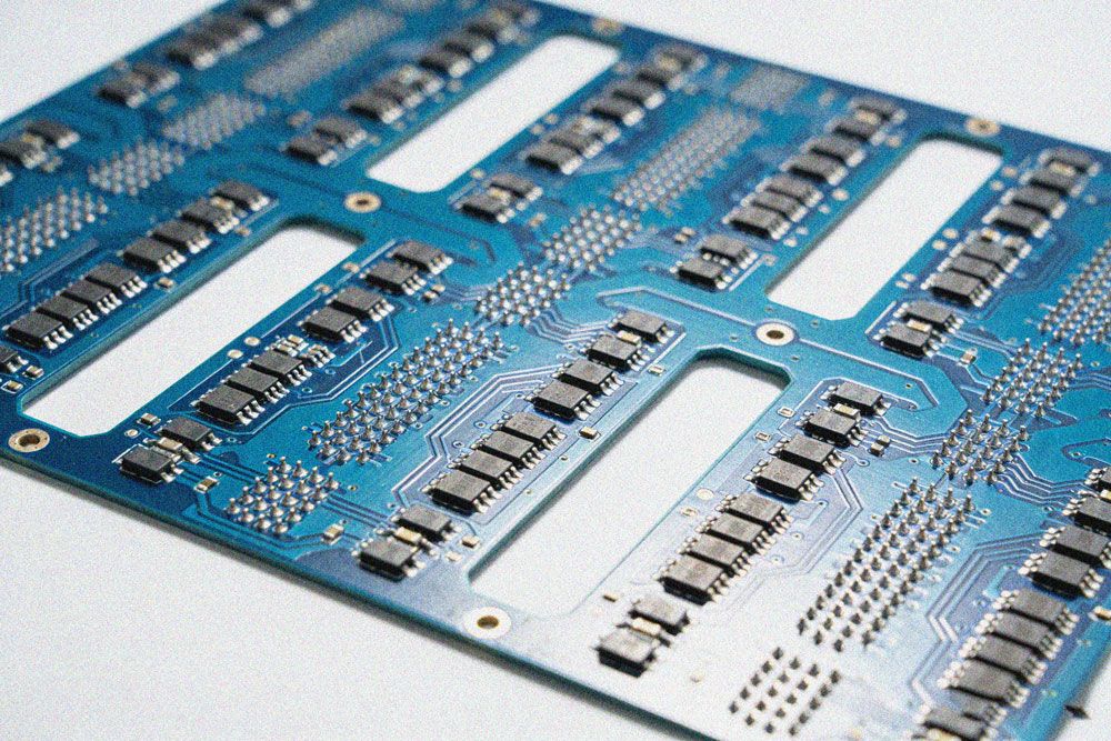
HDI PCB: The Cornerstone and Extension of Advanced Packaging
Whether it's the silicon interposer (2.5D) inside the chip or directly stacked chips (3D), ultimately, they all need to connect to the outside world through HDI PCB or substrate-like circuitry (SLP). HDI technology provides the necessary high-density interconnect capabilities through micro-blind vias, buried vias, and finer lines.
KINGBROTHER's technical capabilities show that its prototyping capabilities in the HDI field can reach 30 layers of any order, and mass production can achieve 26 layers of 4-order HDI, with a minimum linewidth/spacing of 2.0/2.0 mil (prototype). This ability to interconnect any layer is crucial for FC-BGA packaging, which requires complex routing to avoid BGA areas and achieve the shortest transmission path. The "AI Accelerator Card Stacked Via HDI Board" and "11-Order Staggered Via HDI Board" mentioned in the "New PCB Products" document are direct examples of HDI technology serving high-performance computing scenarios. The former uses a two-order stacked via + mechanical blind via design, while the latter even achieves 10-14 order staggered via HDI for high-precision inductor coil control, demonstrating the potential of HDI technology in handling complex structures and high-precision requirements.
Specific Process Challenges of FC-BGA and 2.5D/3D Packaging
When it comes to FC-BGA and 2.5D/3D packaging substrates, the requirements have upgraded from "fine" to "precise."
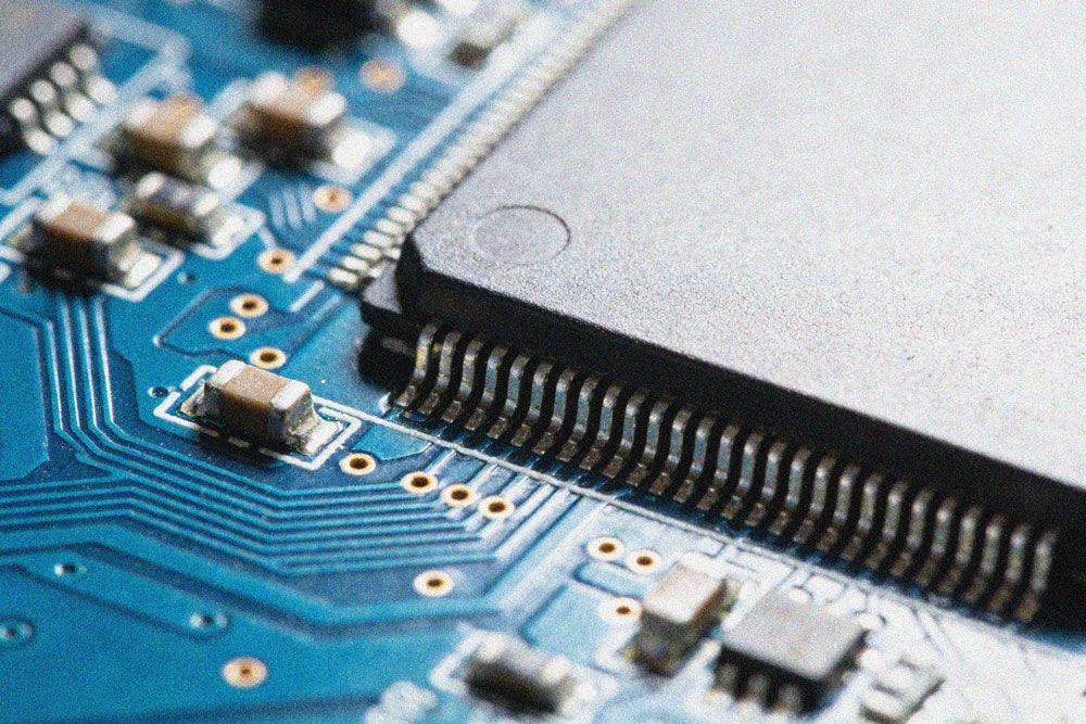
Size and Precision Leap: The unit of measurement for conventional PCBs is "mil" (one-thousandth of an inch), while packaging substrates have entered the "micrometer" era. KINGBROTHER's carrier product process parameters clearly indicate this gap. For example, its "WB-BGA packaging substrate" uses BT material (Shengyi SI10US), with a minimum linewidth/spacing of 25/30µm and a minimum bonding finger spacing of 60µm. The "FC-CSP packaging substrate" requires a linewidth/spacing ≥20/25µm and a solder mask opening of 100µm. These micrometer-level processing precisions are fundamental to ensuring the reliable connection of thousands of microbumps (μBumps) on the chip.
Specialized Material System: High-speed server motherboards may use TU933+ or Panasonic M6, but the packaging substrate has its own unique material tree. In addition to the aforementioned BT material (SI10US), it also requires the use of insulating films (build-up films) such as NBF-T23 for layer addition. This material enables thinner dielectric layers and finer circuitry, adapting to the miniaturization trend of packaging.
Microvias and High Aspect Ratio: The vias in the packaging substrate are more like "microvias". The aperture/hole size of the FC-CSP substrate is 50/120µm. For holes that need to penetrate multilayer substrates, controlling the aspect ratio (the ratio of board thickness to hole diameter) is a significant challenge. Technical documentation mentions that for IC substrates, the minimum laser microvia aperture can reach 50µm, while the maximum aspect ratio needs to reach 25:1 or even 30:1. This requires extremely high levels of drilling and electroplating processes to ensure uniform copper thickness on the hole walls and avoid signal transmission defects or reliability issues.
Collaborative Design: Performance Assurance from Chip to System
AI Computing PCB Design In the era of advanced packaging, early collaboration with chip packaging design is essential. This brings several core design challenges:
Signal Integrity (SI) and Power Integrity (PI): With data rates moving towards 112Gbps (prototype) and even higher, any tiny reflection, loss, or crosstalk can lead to bit errors. KINGBROTHER faced the challenge of 750Gbps high-speed I/O when designing an evaluation board for the NVIDIA Jetson AGX Xavier. Their solution includes using a 10-layer board, strictly controlling the 100Ω differential impedance, planning a four-layer ground plane to provide a low-impedance return path, and using their self-developed KBEDA SKILL tool for early-stage SI simulation. For the packaging substrate, its dense wiring makes crosstalk control more difficult, requiring accurate modeling using 3D electromagnetic field simulation.
Thermal Management: AI chips consume enormous power, and heat is conducted to the substrate through thousands of bumps. The substrate itself must have efficient heat dissipation capabilities. KINGBROTHER showcased technologies such as locally embedded ceramic (thermal conductivity ≥170W/mk) and thermoelectrically separated bump copper substrates in their "High Heat Dissipation Products" presentation. In advanced packaging, it may be necessary to embed microchannels within the substrate or use high thermal conductivity materials to quickly direct heat to the heat sink. Simultaneously, thermal stress can cause a mismatch in the material expansion coefficients, affecting long-term reliability, which needs to be considered during material selection and structural design.
Power Delivery Network (PDN): Instantaneous currents of hundreds of amperes need to be delivered to the chip "calmly." This necessitates extremely low power plane impedance within the substrate, requiring meticulous optimization of decoupling capacitor placement and selection. In the evaluation board example, noise suppression was achieved by placing the power plane adjacent to the ground plane and incorporating a real-time power detection and management module. These approaches are equally crucial in package substrate design.
Advanced packaging of AI chips pushes the technological boundaries of HDI PCBs to their limits, giving rise to a separate AI PCB advanced packaging substrate track. From micron-level circuitry and high aspect ratio microvias to dedicated BT/ABF material systems and deep co-design with SI/PI/thermal management, each aspect presents significant manufacturing and engineering challenges.
KINGBROTHER, leveraging its technological expertise in high-multilayer PCBs, arbitrary-level HDI, substrate manufacturing (such as WB-BGA and FC-CSP), and multi-chip integrated evaluation boards (such as Jetson AGX Xavier), demonstrates its ability to meet these new requirements. Its technology platform demonstrates that, in the prototype stage, it can achieve a signal transmission rate of 112Gbps, a maximum of 72 FR4 layers, and a maximum linewidth and spacing of 2.0/2.0 mil. These capabilities form the foundation for supporting the in-depth development of AI computing PCB design into the packaging field.
In the future, with the popularization of chiplet technology, packaging substrates will undertake more complex heterogeneous integration and interconnection tasks. The ability to connect the entire chain from high-end PCB design and HDI/substrate manufacturing to system-level co-simulation verification will become key to empowering the next generation of AI hardware innovation. This is not merely an upgrade in process technology, but a comprehensive evolution from design thinking to manufacturing systems.
Looking for AI Packaging Substrate Manufacturing?
KingBrother capability highlights:
- ABF / BT substrate
- FC-BGA prototyping
- 30-layer HDI
- 112Gbps SI validation