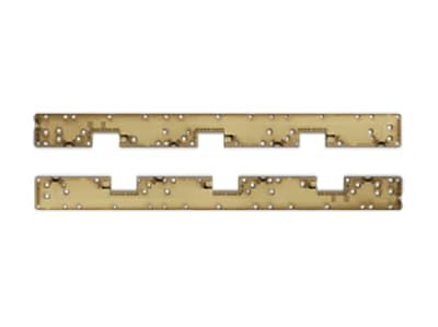
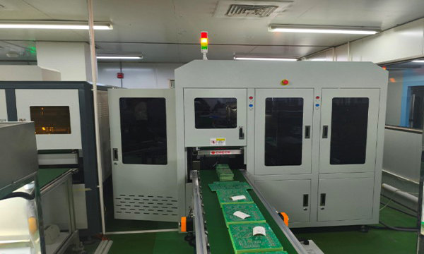
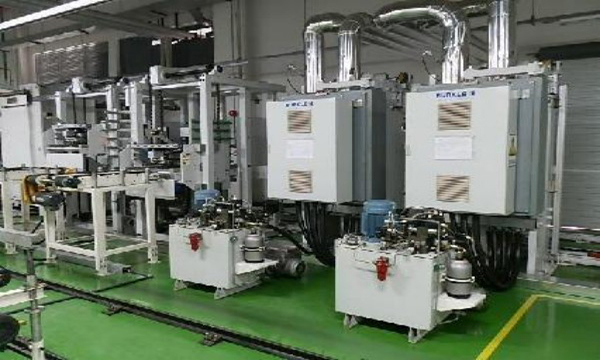
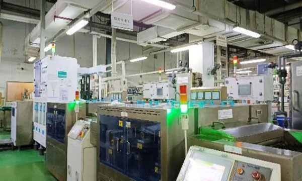
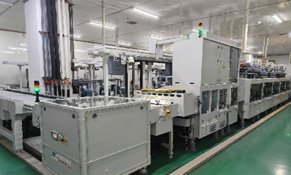
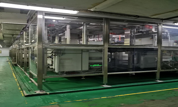
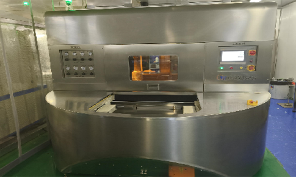


PCB Manufacturing Service
With 29 years of expertise in high-end and specialty PCBs, we deliver reliable and flexible manufacturing solutions. We offer prototyping, quick-turn, and small-to-medium volume PCBs, including multilayer, HDI, high-copper, and rigid-flex boards, backed by a one-stop PCB service that empowers clients across industries, from AI hardware to cutting-edge electronics, to accelerate product innovation and bring ideas to market faster.


