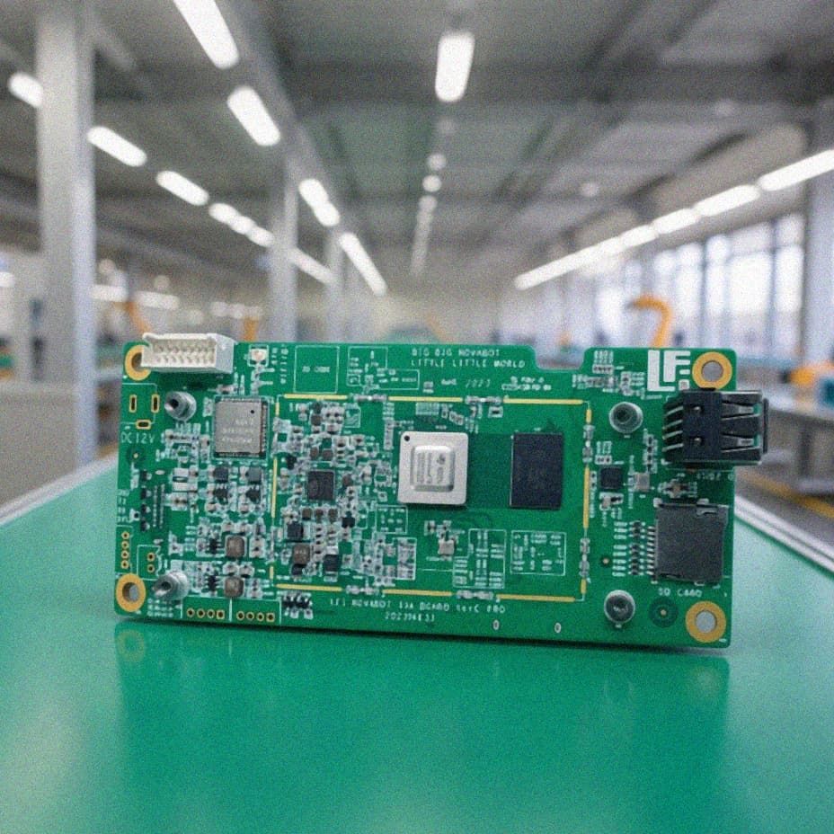
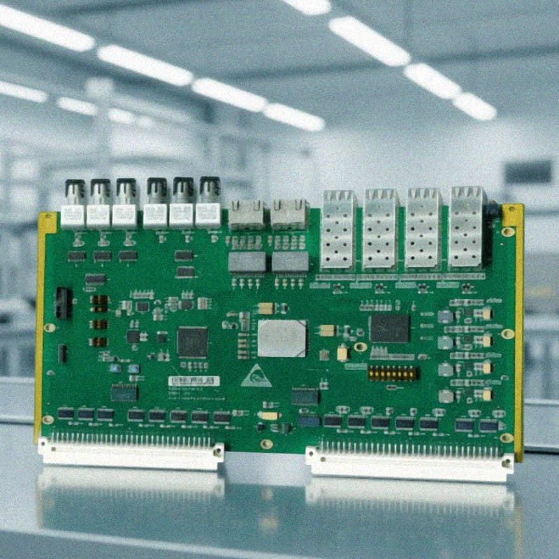
Overview
PCB design is the core foundation of electronic product performance, reliability, and manufacturing feasibility, directly impacting product time-to-market, total production cost, and long-term operational stability. Common design challenges including high-speed signal crosstalk, impedance mismatch, poor thermal dissipation, and lack of design for manufacturing (DFM) consideration often lead to repeated prototype reworks, extended R&D cycles, and unplanned cost overruns for electronic product teams. Our PCB design service adopts a systematic design-oriented approach, covering end-to-end processes from schematic review, stack-up planning, component placement, routing optimization, design verification, to production file output, catering to diverse project requirements from quick turn prototype verification to high-end mass production. We prioritize balancing product functional performance, energy efficiency, manufacturing cost, and production cycle in every design project, delivering optimized, production-ready design solutions that align with both technical specifications and commercial targets.
Technical Capabilities
Our PCB design service covers a wide range of technical scenarios, with capabilities to address complex design requirements for high-performance electronic products:
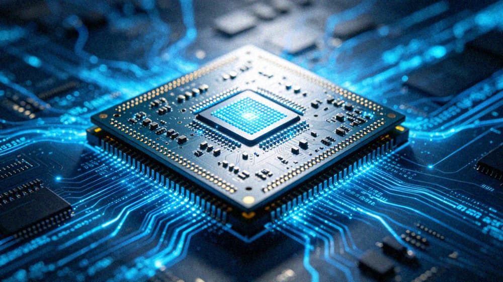
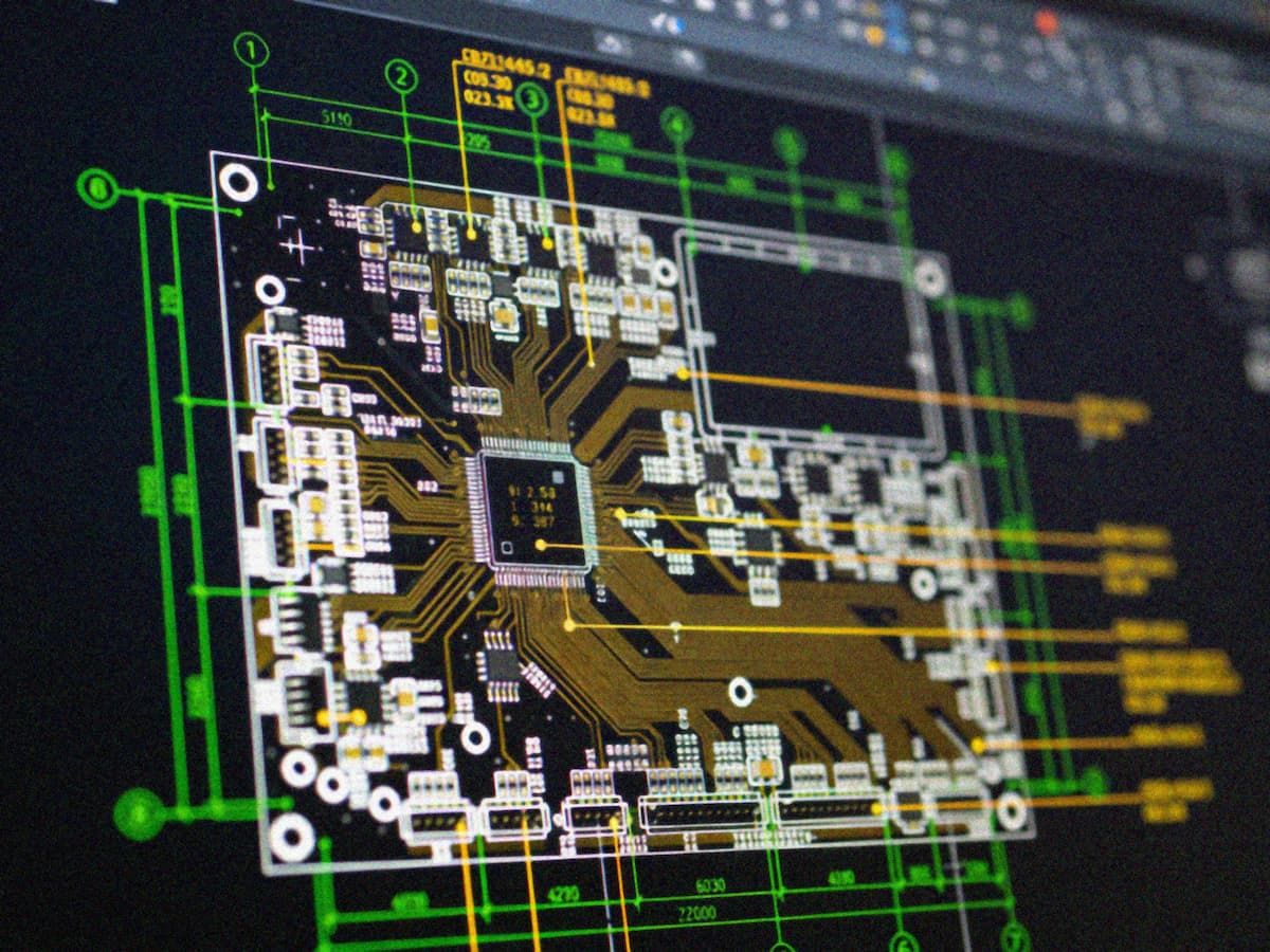
- High-Speed Signal Design Support: We support design and optimization for high-speed signal transmission up to 750Gbps, compatible with common high-speed interface protocols including PCIe 5.0, DDR5, MIPI, 5G NR, and 100G Ethernet. Our design team implements targeted routing strategies, differential pair length matching, and interference shielding measures to minimize signal attenuation, crosstalk, and reflection, ensuring stable transmission for high-density, high-bandwidth product scenarios such as AI computing boards and communication modules.
- Precise Impedance Control: We achieve ±5% high-precision impedance control for common impedance requirements including 90Ω, 100Ω, and 85Ω, adapting to the transmission needs of differential signals, memory interfaces, and high-speed I/O ports. We provide customized stack-up design for 2 to 40-layer PCBs, with configurable independent ground planes and power planes to effectively shield interference between different signal layers, meeting the high-density routing demands of complex electronic products.
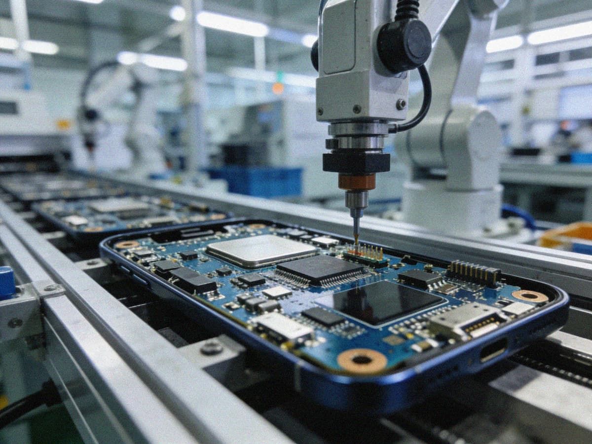
- DFM & DFT Optimization: We integrate manufacturing feasibility checks and testability design into the early stage of the design process, adjusting line width/space, via size, pad configuration, and component placement to align with standard PCB manufacturing and assembly process capabilities. This reduces prototype rework rates by more than 80% compared to non-optimized designs, and shortens the transition cycle from design to mass production. We also add standardized test point layouts according to project requirements, supporting post-production functional testing, reliability testing, and fault diagnosis.
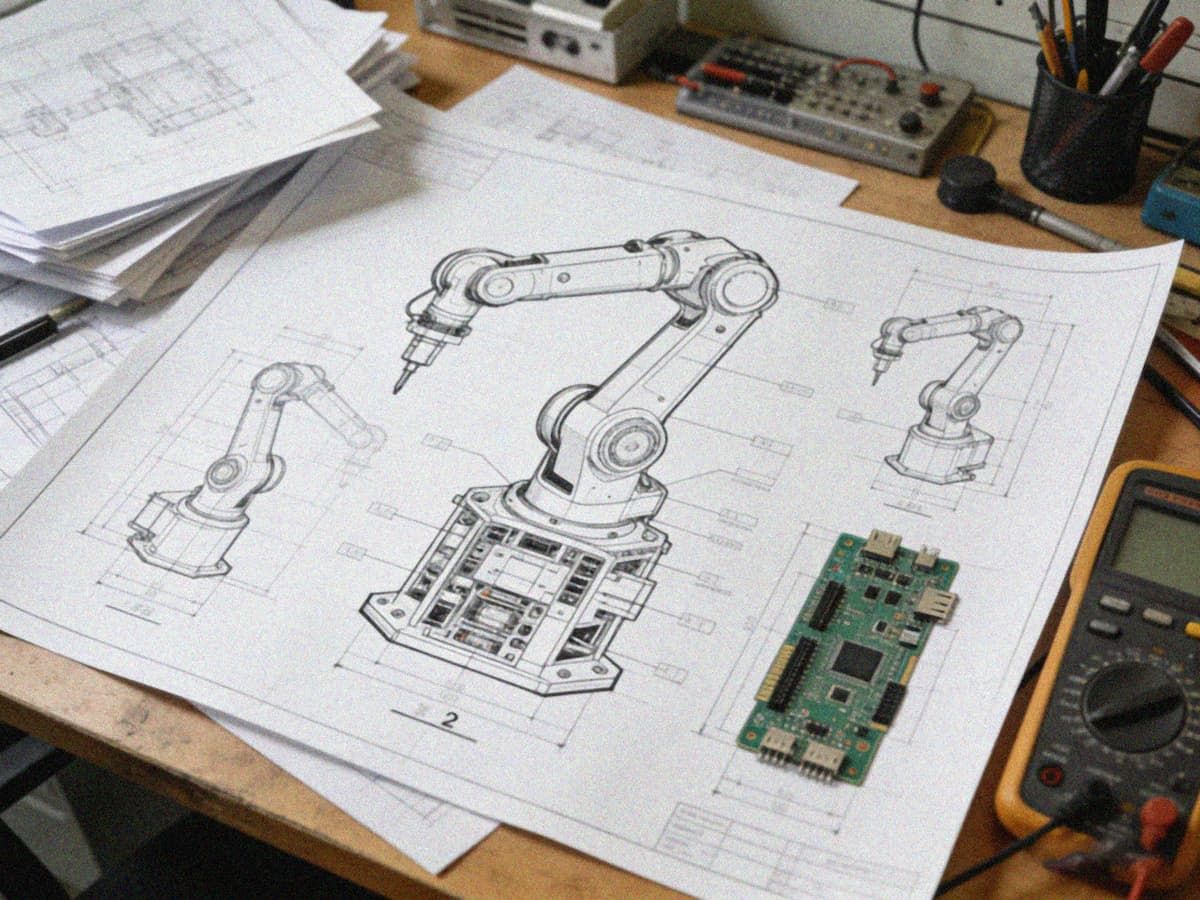
- Quick Turn Prototype Design: We support fast design iteration for PCB prototype projects, delivering optimized, production-ready design files within 24 to 72 hours based on project complexity. Our design process is fully aligned with quick turn PCB manufacturing and assembly workflows, ensuring that prototype designs can be directly put into production without additional adjustments, helping product teams accelerate R&D verification and time-to-market.
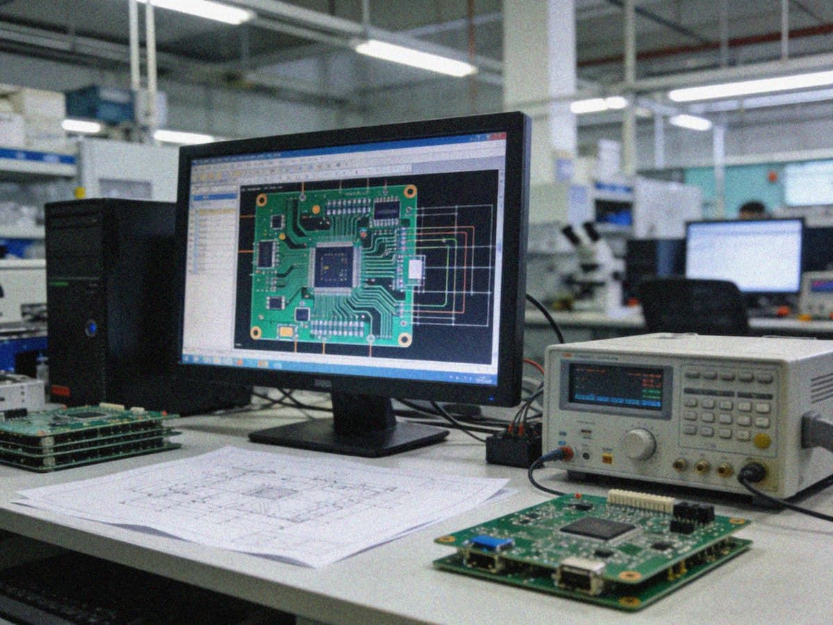
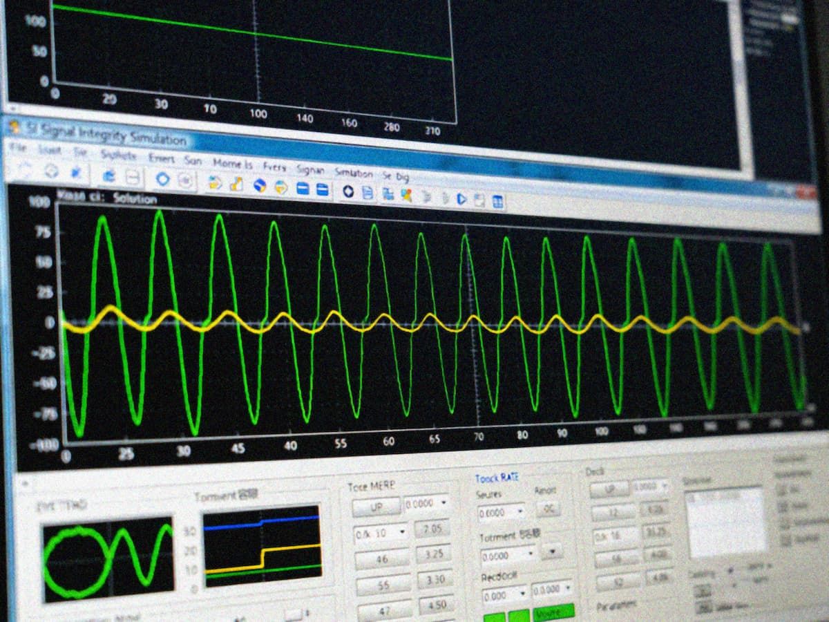
- Multi-Domain Design Verification: We provide full-domain design verification services before design file handover, including signal integrity (SI) simulation, power integrity (PI) simulation, EMC pre-compliance testing, and thermal simulation. These verification steps identify potential performance risks such as voltage drop, signal distortion, and overheating before manufacturing, ensuring that the end product can operate stably across its full operating temperature range and application scenarios.
Quality Standards
All PCB design processes follow strict global industry standards and internal control specifications, ensuring design output consistency and reliability:
- All design workflows adhere to IPC-2221 (generic PCB design standard), IPC-2222 (rigid PCB design standard), and IPC-7351 (land pattern design standard), ensuring compatibility with global PCB manufacturing and assembly supply chains.
- For industry-specific application scenarios, we follow corresponding sector-specific design standards: including AEC-Q100 related design requirements for automotive electronics, ISO 13485 aligned design processes for medical electronics, and IEC 61010 safety standards for industrial electronic products, meeting the compliance requirements of different regulated sectors.
- Every design project goes through at least 3 rounds of independent cross-review by senior design engineers, covering schematic validation, routing rule check, DFM audit, and performance simulation result review, eliminating more than 99% of potential design flaws before file handover.
- All design outputs include a complete, standardized production data package, including Gerber fabrication files, coordinate files, BOM lists, assembly drawings, test specifications, and design specification documents, supporting seamless transition to PCB manufacturing, component sourcing, PCBA assembly, and testing stages without additional data sorting or adjustment.
Applications
Our PCB design service is suitable for a wide range of electronic product scenarios across industries:
- High-performance computing hardware: AI edge computing boards, server motherboards, data center high-speed communication modules, graphics card core boards
- Automotive electronics: autonomous driving domain controllers, smart cockpit core control units, in-vehicle sensor interface boards, battery management system (BMS) control boards
- Industrial electronics: industrial control motherboards, IoT gateway devices, industrial robot core control boards, industrial camera interface boards
- Medical electronics: portable diagnostic equipment, medical imaging processing boards, patient monitoring terminals, medical IoT transmission modules
- Consumer electronics: high-end smart terminal motherboards, wearable device core boards, AR/VR processing modules, high-performance gaming hardware PCBs
- Telecommunications equipment: 5G base station communication boards, optical module interface boards, satellite communication terminal PCBs, private network communication device core boards
Key Advantages
Our PCB design service stands out for its focus on practical manufacturing feasibility and customer value delivery:
- Design-Oriented Optimization Framework: We adopt a systematic design-oriented approach, adjusting design strategies according to project performance targets, budget limits, and production cycle requirements. We provide value-added design recommendations to optimize material selection, stack-up structure, and routing schemes, reducing total product lifecycle cost by 15% to 30% on average without compromising functional performance.
- Full-Chain Process Alignment: Our design specifications are fully aligned with standard PCB manufacturing, component sourcing, PCBA assembly, and testing processes, eliminating cross-stage communication barriers between design and production teams. We ensure more than 99% of design solutions can be directly put into mass production without additional adjustments, reducing coordination costs and production delays caused by design-manufacturing mismatch.
- Flexible Service Scalability: We support flexible service scope adjustment according to customer needs, covering both full turnkey design from schematic development to production file output, and partial design optimization services such as SI/PI tuning, DFM audit, and existing design iteration. We cater to both small-batch prototype design requirements for R&D teams and large-scale mass production design requirements for mature product lines.
- All-Time Technical Support: We provide 7×24 hour technical support and design iteration services, with a 2-hour quick response mechanism for design change requests, quotation inquiries, and technical consultation. We can adjust design schedules according to tight project timelines, supporting fast time-to-market for new electronic products.
Contact Information
If you have customized PCB design service requirements, including high-speed signal design optimization, quick turn prototype design iteration, mass production design validation, or existing design DFM audit, you can reach out to our technical support team for a free project evaluation and customized solution quotation. We provide 2-hour quick quotation response and dedicated technical support throughout the entire project lifecycle, helping you resolve design challenges and achieve project targets efficiently.