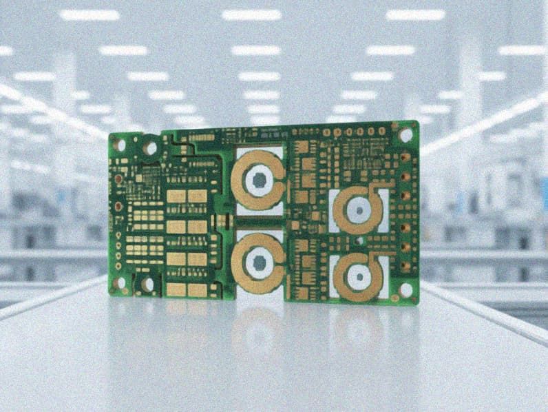
High-Density HDI Board
Product Overview
High-Density HDI boards utilize advanced technologies such as microvias and blind/buried vias to achieve high-density interconnects, enabling more complex routing and higher component integration within limited space. Featuring multi-level micro-blind via structures and high-density routing with line width/spacing down to 2.0/2.5 mil, these boards significantly enhance signal transmission efficiency and overall circuit performance. With their lightweight structure, high reliability, and excellent electrical characteristics, HDI boards are widely used in telecommunications, industrial control systems, and medical electronics—especially in applications requiring high performance and miniaturization.
| Item | Specification |
|---|---|
| Application | High-layer Heavy Copper HDI Board / Power Module |
| Material | S1000-2 |
| Layers | 12L |
| Copper Thickness | 3 oz (inner & outer layers) |
| Minimum Line Width / Space | 4.5 mil / 4.5 mil |
Share To:
Our Capabilities
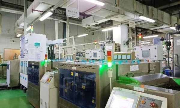
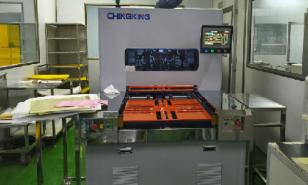
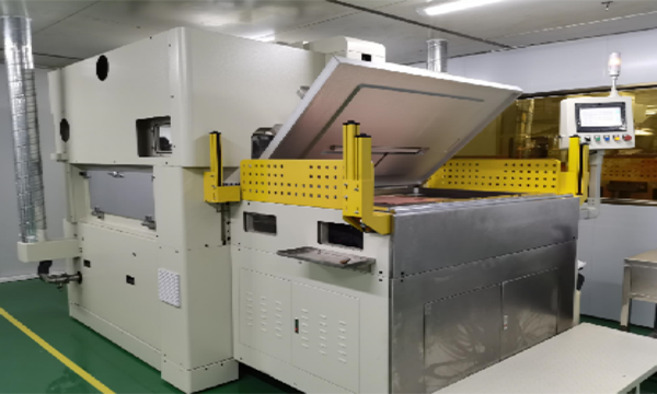
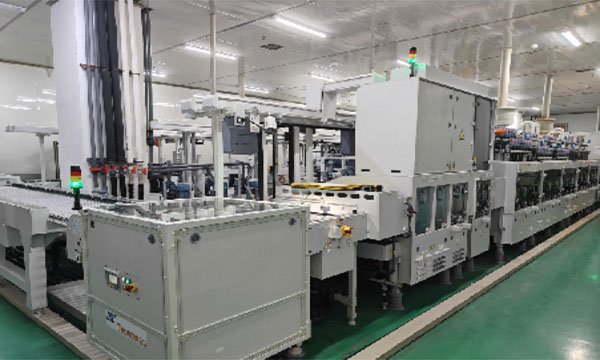
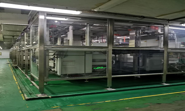
Production Equipment
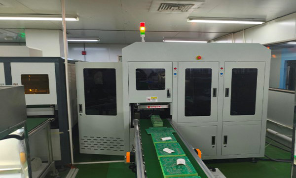
AVI visual inspection machine
Boke Precision Vacuum Laminator
Ceramic grinding machine
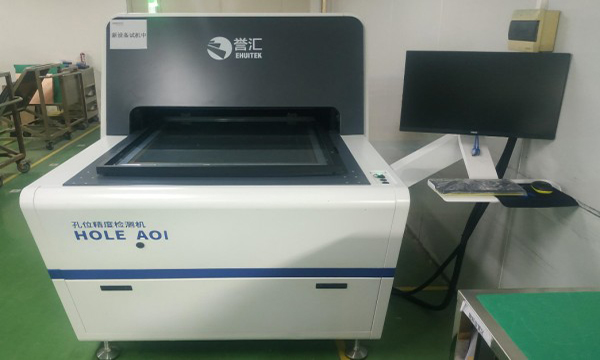
Hole position accuracy testing machine
Lamination hot melt machine
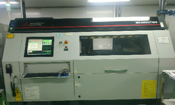
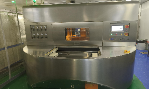
Mitsubishi 6th Generation Laser Drilling Machine
Vacuum Resin Plug Machine
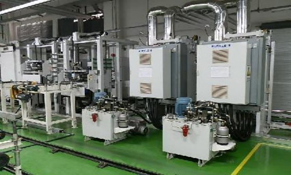
Vacuum two-fluid etching machine
VCP continuous electroplating line