The global "artificial intelligence +" policies continue to intensify, and the demand for intelligent computing centers, edge AI devices and high-end servers is experiencing explosive growth. The supply-demand pattern of computing power is undergoing a drastic transformation. Industry analysis institution Epoc AI shows that global AI computing power is iterating at a rate of doubling every 7 months, with an annual compound growth rate of over 300%. Its growth curve is much steeper than Moore's Law. This "computing power arms race" led by giants such as NVIDIA and Google is placing extreme performance requirements on the underlying supporting PCB and server motherboards. As the core carrier of electronic systems, PCBs and high multi-layer server motherboards in AI computing scenarios need to simultaneously meet multiple demands such as high concurrency, large bandwidth, and strong heat dissipation. The rationality of their design and manufacturing accuracy directly determine the stability and iteration efficiency of computing power equipment.
The extreme demands of high computing power scenarios are causing PCBs and server motherboards to encounter multiple technical challenges. In terms of performance, the high-frequency signal transmission requirements of AI computing keep pushing the limits. Current mainstream devices have explicitly stated a demand for a 112Gbps rate. However, traditional PCBs are prone to signal attenuation and reflection issues. At the same time, the high-density integration of chips leads to heat accumulation, with the core area temperature often exceeding 85℃, severely affecting the stability of operation. In terms of integration difficulty, high multi-layer motherboards (16–32L) have become standard equipment for high-end computing power devices. However, their high-density interconnection design faces the problem of electromagnetic interference (EMI). The traditional process impedance control tolerance is mostly above ±10%, making it difficult to meet the requirements for high-speed signal transmission. Moreover, the line width and spacing need to be compressed to below 0.08mm, posing strict challenges to manufacturing precision. The contradiction between cost and cycle is also prominent. Core materials for high-end PCBs, such as HVLP copper foil and ABF substrate, have long relied on imports. In addition, the complex high multi-layer board process leads to an industry average production yield of only 85%, resulting in high procurement costs and delivery cycles typically lasting 30–45 days. More critically, computing power devices are often in complex industrial environments such as high temperatures, high humidity, and vibration. Traditional PCBs have insufficient corrosion and aging resistance, with equipment failure rates exceeding 5%, making it difficult to meet the long-term lifecycle requirements of 10 years or more.
To address these challenges, an integrated approach covering design simulation, material selection, manufacturability optimization, and mass production validation is required.
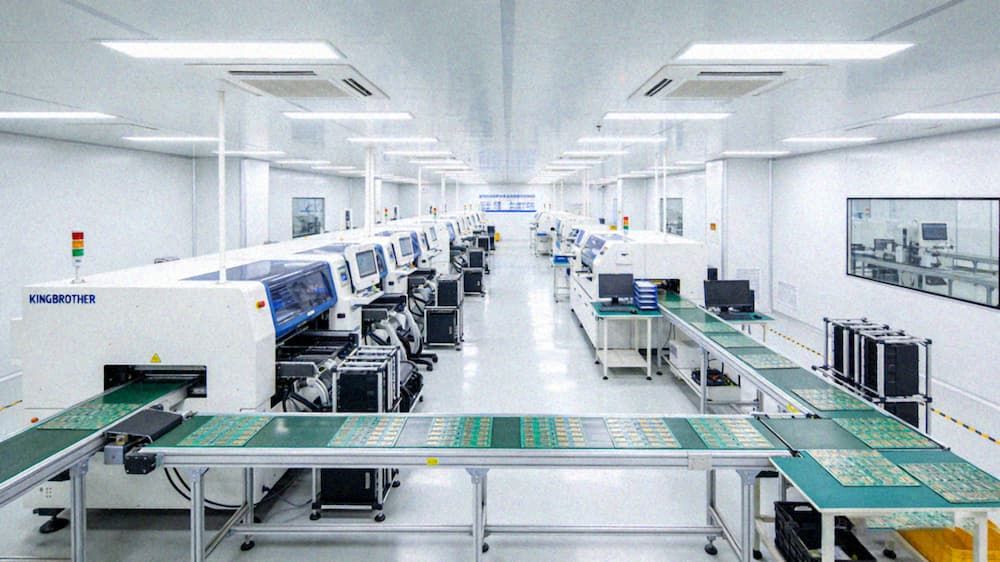
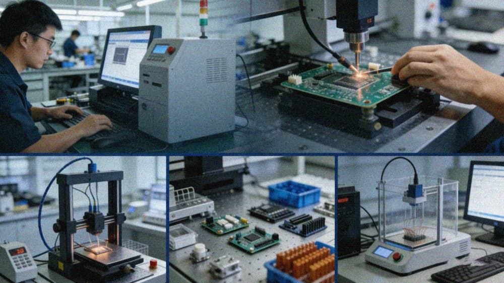
This is where KINGBROTHER’s IPDM one-stop solution is designed to work. With 29 years of experience, KINGBROTHER has developed an IPDM one-stop solution centered on integrated product design (IPD), integrated product manufacturing (IPM), and printed circuit boards (PCB) to address these pain points. Through six technical platforms including IDH, CAD, and PCBA, it forms a full-process closed-loop to provide empowerment. This solution is deeply adapted to high computing power scenarios and has achieved a 72-layer 112Gbps high-speed PCB design capability. The modular reuse rate is 68%, far exceeding the industry average of 35%. At the same time, with a 3.27 million certified material library and mature EMC optimization solutions, the product EMC pass rate has been increased to 98.5%. The overall success rate of the solution has increased by 35% compared to the industry average. Unlike traditional segmented services, KINGBROTHER intervenes in the demand analysis stage and uses pre-production simulation and process optimization to avoid design and manufacturing connection contradictions in advance, achieving efficient transformation from R&D to mass production.
Core Technology Breakthroughs
KINGBROTHER has developed a differentiated technical system for AI computing PCBs and high multi-layer server motherboards.
AI Computing PCB
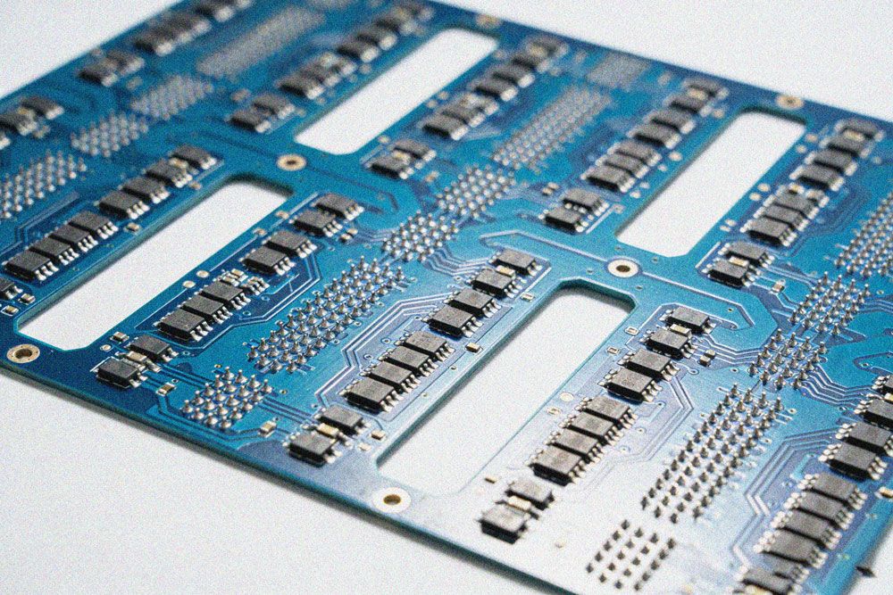
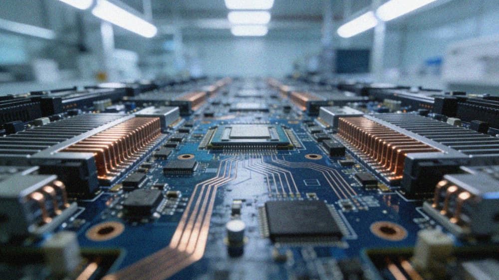
The AI computing PCB focuses on three core dimensions: heat dissipation, signal integrity, and material compatibility. It adopts a thick copper (≥10 OZ) and buried copper block composite process, combined with high-density heat dissipation holes and full-board copper filling design, and selects aluminum-based or ceramic-based substrates. This can increase the chip's heat dissipation efficiency by 40%, effectively solving the problem of high-temperature accumulation. In terms of signal transmission, through precise wiring of differential pairs and impedance matching technology, the impedance control tolerance is reduced to ±5%, ensuring stable 112Gbps transmission across PCIe 5.0 links without repeated tuning. Combined with SI/PI joint simulation tools, it minimizes signal interference and reflection, stabilizing the support for 112 Gbps high-speed transmission, fully compatible with PCIe 5.0 and above standards. In terms of material selection, high-speed and low-loss materials such as TU933+ and SI-610 are prioritized. These materials have a dielectric constant controlled within 3.2–3.8 and dielectric loss tanδ ≤ 0.004, which can significantly reduce high-frequency signal attenuation. At the same time, high-temperature-resistant FR-4 substrates with a Tg ≥ 170°C are selected to ensure structural stability in high-temperature scenarios.
High Multi-layer Server Motherboard
The high multi-layer server motherboard has achieved breakthroughs in the design of the layer structure, process precision and domesticization adaptation. The layer design can flexibly cover the mainstream demands of 16–32L, and in the sample stage, 72-layer technical verification has been achieved. It adopts HDI any-layer interconnection technology, controlling the accuracy of blind-buried holes at 0.05mm. Through the combination of "blind holes + buried holes + through holes" interconnection method, it can increase the line density by 50% within the same area, perfectly adapting to the wiring requirements of chips with over 1000 pins such as FPGAs. In terms of process, it integrates metallization slot holes, multiple back drilling and high-density resin filling technology, breaking through the bottleneck of multi-layer board interconnection, controlling the minimum line width/spacing at 4.5/2.5 mil, and improving the current carrying capacity by 30% compared to the industry average. In terms of domestic adaptation, it follows the wave of core material domestic substitution led by HVLP copper foil, and is compatible with products from domestic suppliers such as Tongguan copper foil and Defu Technology. The core component domestic substitution rate exceeds 80%, and it can be matched with domestic chip platforms such as Rockchip Microelectronics, Anlu Technology and Horizon. This effectively reduces the risk of supply chain dependence and addresses issues such as import material price hikes and supply fluctuations.
To visually demonstrate the technical advantages, the following is a comparison of the core parameters of the KINGBROTHER solution with the industry average:
| Technical Indicators | Industry Average | KINGBROTHER Solution Level | Applicable Scenarios |
|---|
| Maximum PCB Layers | 24L (Commercial mainstream) | 32L (Stable mass production, samples up to 72L) | AI computing servers, high-end computing equipment |
| Signal transmission rate | 56Gbps | 112Gbps (Stable support) | High bandwidth data centers, 400G optical modules |
| Impedance control tolerance | ±10% | ±5% | High bandwidth AI signal transmission, PCIe 5.0 interface |
| Mass production delivery cycle | 30–45 days | 15–25 days | Small batch trial production, large batch mass production projects |
| Product mass production yield | 85% | 98% | High multi-layer server motherboard mass production |
| Domestic substitution rate of HVLP copper foil | Less than 20% (Expected 40% in 2026) | 80%+ | Domestic demand for computing equipment projects |
The abundant implementation cases have verified the practicality and reliability of the solution.
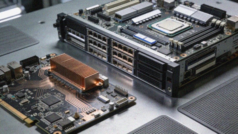
Case Study: 32-layer AI Server Motherboard with NVIDIA Jetson Platform
A leading AI computing enterprise once faced an urgent demand for a 32-layer server motherboard, which needed to be compatible with the NVIDIA Jetson Orin NX chip, with a signal transmission rate of ≥100Gbps, and a requirement for a production cycle of ≤30 days. The core difficulties were concentrated in three dimensions: 32-layer high-density interconnection, electromagnetic interference suppression, and chip heat dissipation optimization. KINGBROTHER addressed this demand by selecting TU933 + high-speed low-loss materials, using HDI arbitrary-layer interconnection and multiple back-drilling processes, combining a "thick copper + heat dissipation holes + copper filling" composite heat dissipation system, and precisely matching domestic HVLP copper foil and components through the KBOM platform, achieving an 85% domestic substitution of components. The final delivered solution improved signal transmission stability by 35%, reduced the chip working temperature by 25°C, achieved a mass production yield of 98.2%, shortened the delivery cycle to 22 days, which was 8 days ahead of the customer's expectation, reduced the procurement cost by 18%, and successfully supported the customer's computing equipment to be launched quickly and iteratively.
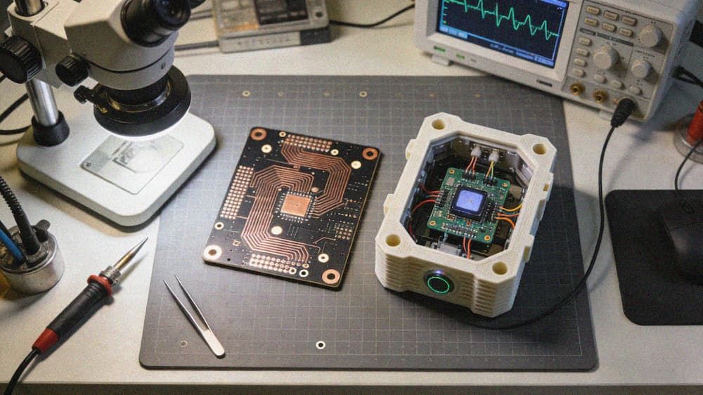
Case Study: An edge AI Controller for Industrial Application
In the edge AI scenario, an industrial customer needs to develop an edge AI controller. The requirement is that the device should be able to withstand a wide temperature range of −20℃ to 60℃, integrate multiple sensor interfaces, and have strong anti-electromagnetic interference capabilities. KINGBROTHER adopts a combined rigid-flexible board design. Through the gold plating process, the PCB's corrosion resistance and wear resistance are enhanced. Combined with the three-proof coating treatment, the adaptability to extreme environments is improved. At the same time, by leveraging EMC simulation tools, the wiring structure is optimized, dividing independent power zones and grounding isolation strips, reducing power noise coupling by 40%. After the implementation of the solution, the equipment failure rate has decreased from the original 6.2% to 0.8%, fully meeting the requirements of complex industrial scenarios such as smart logistics and security patrol. It has been deployed and applied on a large scale.
The core value of the KINGBROTHER solution lies in providing multiple enhancements such as cost reduction, speed improvement, quality enhancement, and efficiency increase for high-performance computing projects. In terms of manufacturability optimization, it utilizes a 2368-rule database to conduct pre-production simulation manufacturing, enabling the early detection of design flaws such as wiring and stacking, thereby reducing production anomalies by 60% and avoiding subsequent rework losses. In terms of reliability verification, it leverages CNAS/CMA qualified laboratories to conduct comprehensive tests including high and low temperature cycles, vibration and shock, and wet heat aging, ensuring that the product lifespan is extended to over 10 years, meeting industrial and military-grade reliability standards. The customization capability can precisely match the different layer requirements of 16–32L, providing personalized process solutions for special demands such as heat dissipation and high-frequency signals, without requiring customers to compromise on performance requirements. In terms of cost and cycle control, it reduces the procurement cost by 15–20% through the substitution of domestic components, compresses the production cycle to 60% of the industry average, and helps customers accelerate product launch speed by 2 times, seizing the initiative in the computing arms race.
Currently, the global demand for AI computing power is continuously surging. The demand for AI-compatible PCBs in China is expected to reach 150 billion yuan by 2026, while the existing production capacity is only 120 billion yuan. The 30 billion yuan supply-demand gap provides a broad space for enterprises with core technologies. KINGBROTHER has solved the core pain points of PCBs and server motherboards in high computing power scenarios through technological breakthroughs. Through the IPDM one-stop service system, it achieves comprehensive value such as "performance meeting standards, cost controllable, cycle shortened, and reliability improved". It has become a preferred partner for scenarios such as AI computing power servers, intelligent computing centers equipment, and edge AI controllers.
In the future, KINGBROTHER will continue to focus on the research and development of high-speed PCB and high multi-layer motherboard technologies, keeping up with technological trends such as HVLP5 copper foil and M9-level high-speed materials. It will further enhance its domestic adaptation capabilities and high-frequency signal processing levels. In response to the personalized needs of AI computing scenarios, KINGBROTHER can provide free demand assessment, solution design, and sample testing services, helping enterprises quickly break through the technical bottlenecks at the bottom layer of computing equipment. If you need exclusive AI computing PCB design or high multi-layer server motherboard solutions, you can contact the KINGBROTHER technical team at any time to jointly seize the new opportunities in the era of high computing power.