


Yes. Our PCB design services offer scalable solutions for prototype PCB assembly and high-volume PCB manufacturing, ensuring quality and efficiency at every stage of production.
View More >>Electronic Manufacturing Service
Our ServiceServices we're offering
Services we're offering
to our customers
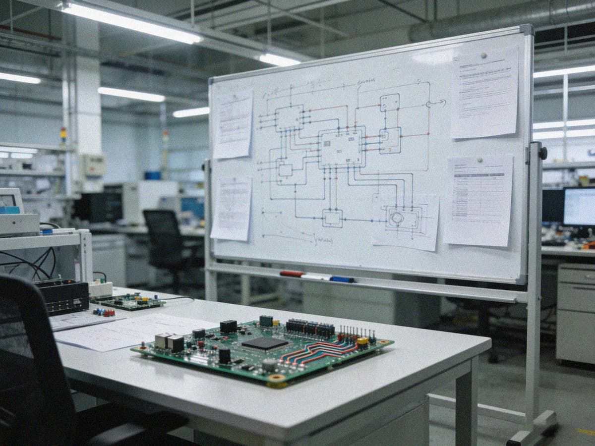
Reliable AI hardware solutions with full-lifecycle supply chain support. We provide highly reliable electronic manufacturing services. Our integrated PCBA, BOM management, NPI engineering and advanced failure analysis to guarantee reliable performance at every stage.
Service Overview
Core service content
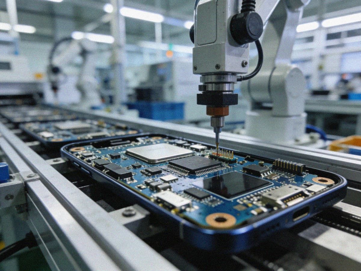
PCBA Services
- Core processes: THT, SMT, mixed assembly process, automatic spraying, automatic dispensing, 3D assembly, ICT testing, aging testing
- Specialized processes: Ai computing power board welding, selective wave soldering, high-reliability nitrogen reflow soldering
BOM Service
- Core directions: Customized materials, R&D material procurement, R&D BOM agency procurement, material substitution and verification, material localization, component agency procurement, BOM order matching, AI material selection
- Solutions: BOM solutions, hardware integration solutions, reliability solutions
Electronic Engineering Services
- Core capabilities: DFX simulation design, DFM (Design for Manufacturability), reliability testing, material handling solutions, reliability engineering solutions, hardware circuit optimization design
Choose our advantages
Accelerate R&D and prototyping
- One-stop integrated design and manufacturing solution: covering the entire process from rapid prototyping, component procurement, PCBA to testing
- Supply Chain Assurance: An efficient BOM supply chain platform, cooperation with over 2,000 global brands and agents, and tens of millions of industry BOM data ensure stable supply and controllable costs
Facilitate the verification and application of new products
- Risk Management and Control: Automated DFX simulation capabilities enable rapid diagnosis of product risks, enhancing product quality and reducing manufacturing costs
- New Product Incubation: Pipeline-style new product incubation capabilities, NPI (New Product Introduction) standardized management, accelerating the verification and market launch cycle of new products
One-stop service ensures bulk supply
- Response efficiency: 7* 24-hour rapid response
- Production layout: 5 major manufacturing bases (Huizhou, Xi 'an, Hangzhou, Chengdu, Shenzhen), over 20 advanced production lines
- Quality Control: QMS quality Management "Six Checkpoints", comprehensive quality assurance system
Details of manufacturing capacity
Processing Technology Capacity Table
| Project | Conventional Process | Unconventional Process | ||
|---|---|---|---|---|
| SMT process | Minimum PCB size | L≥50mm, W≥50mm | Minimum PCB size | L<50mm, W<50mm |
| Maximum PCB size | L≤450mm, W≤400mm | Maximum PCB size | L≤800mm, W≤450mm | |
| Component thickness (T) | 0.5mm≤T≤3mm | Component thickness (T) | T<0.5mm, T>3mm | |
| Minimum package of the device | 0201 (0.6mm*0.3mm) | Minimum package of the device | 01005 (0.3mm*0.2mm) | |
| Maximum device size | SMD≤200mm*125mm | Maximum device size | SMD>200mm*125mm | |
| Maximum thickness of the device | T≤15mm | Maximum thickness of the device | T>15mm | |
| Minimum PIN Pitch for multi-pin classes such as QFP, SOP, and SOJ | 0.35mm | Minimum PIN pitch for multi-pin classes such as QFP, SOP, and SOJ | 0.3mm≤Pitch<0.35mm | |
| Minimum Pitch for CSP and BGA | 0.35mm | Minimum pitch for CSP and BGA | 0.3mm≤Pitch<0.4mm | |
| DIP process (wave soldering) | Minimum PCB size | L≥50mm, W≥50mm | Minimum PCB size | L<50mm |
| Maximum PCB size | L≤500mm, W≤400mm | Maximum PCB size | L<800mm, W≤400mm | |
| Minimum PCB thickness | T≥0.5mm | Minimum PCB thickness | T<0.5mm | |
| Maximum thickness of PCB | T≤5mm | Maximum thickness of PCB | T>5mm | |
| Conformal coating process | Temperature resistance range | -40℃≤T≤120℃ | Temperature resistance range | -50℃≤T≤150℃ |
| Coating thickness | 25um≤T≤50um | Coating thickness | T>50um | |
| Flying probe testing procedure | Height on the upper side of the device | H≤60mm | Height on the upper side of the device | H>60mm |
| The height under the device | H≤120mm | The height under the device | H>120mm | |
| PCB thickness | T≤5mm | PCB thickness | T>5mm |
Engineering and Technical Capability Table
| Business Competence | Sub-business competence | Technical competence | Remarks |
|---|---|---|---|
| Material reliability | Component selection | Multi-dimensional component selection | Procureability, cost-effectiveness, sustainability |
| Component substitution | Compatibility substitution or functional substitution | Functional substitution | |
| Component inspection | Component agency inspection and secondary screening | Component quality assurance | |
| Design reliability | SCH optimization | SCH design, Modification, Optimization, Standardization | / |
| PCB Optimization | Layout, routing, Impedance, and packaging optimization | / | |
| Reverse engineering | SCH, PCB, BOM reverse engineering | / | |
| Structural optimization | Design of device or housing structure drawings | / | |
| Test reliability | White-box testing/flying probe testing | Through and short circuits, signal testing | / |
| Performance testing | Design and Testing of functional fixtures | / | |
| DFX design | EBOM design | DFP design | PLM |
| PCBA simulation | DFA simulation | DFX | |
| Reliability testing | Environmental testing | High temperature, low temperature, temperature cycle, rapid temperature change, thermal shock, high-temperature aging, salt spray, etc | / |
| Mechanical testing | Vibration, drop, etc | / | |
| Electrical testing | Impedance, withstand voltage, leakage current, insulation resistance, ion migration, function and other tests | / | |
| Material testing | Coefficient of thermal expansion CTE, glass transition temperature Tg, ductility, peel strength, etc | / | |
| Failure Analysis | Product Failure Analysis | Analysis of Product Failure Mechanisms and root Causes | Metallographic secturing, Electron microscopy (including Energy Dispersive spectroscopy) |
| Device failure analysis | Analyzing the mechanism and root cause of device failure | Laser unpacking, acoustic scanning |
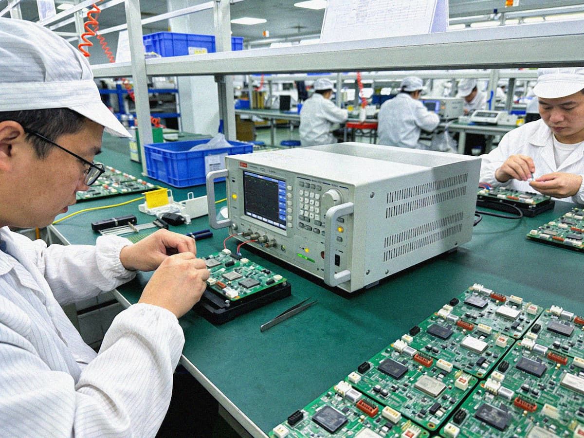
Intelligent production and inspection equipment
Production equipment
3D AOI equipment, surface mount technology (SMT) placement machines, ten-zone lead-free reflow ovens, solder paste printing equipment, DIP wave soldering production lines, conformal coating equipment
Testing Equipment and Qualifications
- Core testing equipment: SEM&EDS (scanning electron microscope and energy Dispersive spectrometer), rapid temperature change chamber, TMA thermomechanical analyzer, universal material testing machine, laser opening machine, C-SAM (Acoustic Scanning microscope)
- Qualification Certification: Laboratory Accreditation Certificate of China National Accreditation Service for Conformity Assessment (CNAS) (Registration Number: CNAS L10908), in compliance with ISO/IEC 17025:2017 standard
Share To:
SolutionsServices Need
Services Need
Well-Matched Solutions
Our faqs
Frequently Asked Questions.
- Can your EMS services handle both prototype and large-scale PCB production?
- Do you assist with PCB layout and design optimization?
Yes. We specialize in PCB design and layout services and incorporate design for manufacturing(DFM) principles to optimize layouts, reduce costs, and improve production workflows, ensuring that your PCB project runs smoothly and efficiently.
View More >> - Do you offer BOM services for EMS manufacturing?
Yes. We provide complete Bill of Materials (BOM) service support, including material selectionand sourcing, to streamline your production process and enhance EMS manufacturing efficiency.
View More >> - How do we handle urgent production orders?
We have a flexible production line and rapid response mechanism to handle urgent productionorders. By optimizing production scheduling and overtime arrangements, we ensure thatproduction tasks are completed in the shortest possible time.
View More >> - How do we support the client during the project?
We assign a dedicated sales manager to each project, providing support from design to delivery. The sales manager maintains close communication with the client to ensure that the project isprogressing as planned and that any questions or needs of the client are addressed in a timely manner.
View More >> - How do you ensure quality in PCB manufacturing?
To guarantee our reliability and performance, we rigorously employ advanced techniques in ourPCB design services, adhering to international standards and performing rigorous electronicengineering and testing. We are certified with ISO 9001, ISO 50001, ISO 45001, ISO 14001, ISO 13485, IATF 16949, ROHS, UL, COC and AEO. Whether it is a flexible PCB, multilayer, HDl, metal board, rigid-flex, or optical communication PCBmanufacture, we ensure every product meets the highest quality benchmarks.
View More >> - What about our PCB production equipment?
We possess advanced production equipment in key processes, ensuring that product precision and consistency meet the optimal state required by the market demands. For instance, all inner and outer layer circuits are produced using LDI, and we have the most advanced Mitsubishi laser drilling machines and laser blind hole copper filling VCP for creating mechanical
View More >>


ABOUT OUR COMPANY
Hardware Solution and Manufacturing Service Provider
Founded in 1997 and headquartered in Shenzhen, KINGBROTHER specializes in electronic interconnection technologies and hardware innovation. We focus on electronic product R&D, AI hardware solutions, engineering services, integrated design and manufacturing, and supply chain capabilities to deliver comprehensive PCB manufacturing, IPD (Integrated Product Development), and EMS services.
We are committed to becoming a world-class AI hardware solutions and manufacturing service provider, offering one-stop solutions for AI robots, industrial control, medical devices, new energy, and automotive electronics, helping our customers accelerate innovation and bring products to market faster.
We bridge R&D to mass production with integrated capabilities:
Precision-Driven System Design to Accelerate Your Success
We adhere to systematic design as our foundation, offering hardware, software, and industrial design services. With 6 self-owned design centers and a knowledge base including 3.27 million certified materials and 2,368 DFI rules, we significantly reduce design iterations by 60-80% and increase customer project success rates by 35%.

End-to-End Technical Integration for Unbroken Innovation
We have built an integrated technology chain from IC design IPD and PCB to integrated product manufacturing IPI. With 300+ technical solutions and over 2,500,000 product models and project verifications, we achieve closed-loop collaboration and optimization throughout the hardware innovation process.

Rigorous Engineering for Uncompromising Product Integrity
Through strict QIS quality management systems and full-chain engineering empowerment via DF8, failure analysis, and process control, we eliminate 90% of pad defects and 70% of assembly risks, ensuring product safety for our customers.

Agile Manufacturing and Supply Chain for On-Demand Fulfillment
Leveraging 5 IPI smart manufacturing bases and a cloud alliance of over 100 factories, we have established a flexible production system for small-batch, multi-batch needs. Our mature global supply chain ensures quick response and delivery, especially in component procurement.

Services
We provide services to 20,000+ clients
The Choice of Dozens of Fortune 500 Companies.

PCB Manufacturing Service
With 29 years of expertise in high-end and specialty PCBs, we deliver reliable and flexible manufacturing solutions. We offer prototyping, quick-turn, and small-to-medium volume PCBs, including multilayer, HDI, high-copper, and rigid-flex boards, backed by a one-stop PCB service that empowers clients across industries, from AI hardware to cutting-edge electronics, to accelerate product innovation and bring ideas to market faster.

Electronic Manufacturing Service
Reliable AI hardware solutions with full-lifecycle supply chain support. We provide highly reliable electronic manufacturing services. Our integrated PCBA, BOM management, NPI engineering and advanced failure analysis to guarantee reliable performance at every stage.

Electronic Product Design Service
We focus on independent design house (IDH) and CAD design, providing AI hardware solutions and covering services such as hardware design, software design, industrial design, and EDA development.
Our Solutions
Full-Stack Electronics Solutions
100% Complete & Professional Solutions: From Design to Manufacturing.
Contact us