Behind the hype, the bottleneck in mass production has always constrained the pace of industrial implementation. The contradiction between high computing power requirements and low power consumption control, the conflict between miniaturization integration and multi-module compatibility, the problem of meeting reliability standards under complex working conditions, as well as the high costs and lengthy R&D cycles caused by reliance on imported components, all these have become obstacles for most enterprises to achieve large-scale production. And the PCB design of AI embedded systems, as the "nerve center" of the core hardware of humanoid robots, its design level directly determines the computing response speed, operational stability and production economy of the robot. It is also the key to solving the aforementioned pain points.
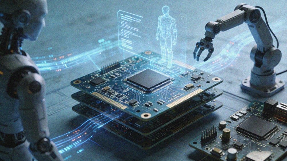
The era of mass production of humanoid robots has arrived, and PCB design has become the key breakthrough point.
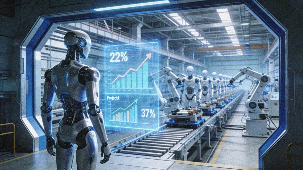
The dual impetus of policy benefits and technological innovation is driving the humanoid robot industry to accelerate its entry into the stage of large-scale mass production. The national "Artificial Intelligence +" action plan clearly includes intelligent robots in the key areas of focus, and the "Belt and Road" intelligent computing solution's overseas export benefits have also been added. The proportion of China's humanoid robot-related industries in the global market has exceeded 22%, and the number of overseas intelligent computing center implementation projects has increased by 37%. From the perspective of industrial practice, the T1 humanoid robot showcased at the Zhongguancun Forum has achieved batch delivery, and the general embodied intelligence platform "Huixi Kaowu" has achieved compatibility and adaptation for multiple configurations of robots, marking the transition of human-machine collaboration from the laboratory to industrial application. The latest industry report from Microsoft states that by 2025, AI agents will cover 15% of industrial physical tasks, ranging from precise assembly to intelligent inspection, and the application scenarios of humanoid robots continue to expand.
Comparison Table of Core Pain Points in Mass Production of Humanoid Robots and PCB Design Solutions
Based on mass-production humanoid robot projects, the following table summarizes the key bottlenecks and corresponding PCB design strategies.
| Mass Production Challenges | Specific Manifestations | AI Embedded System PCB Design Solution |
|---|
| Performance bottleneck | Insufficient computing power leads to task processing delays, distorted high-speed signal transmission, and difficult to meet the requirements of working conditions in terms of battery life | Adopting GPU/FPGA/ARM heterogeneous architecture, supporting 112Gbps high-speed differential signal transmission, and combining with dynamic power regulation circuits to achieve precise balance between computing power and energy consumption |
| Integration challenge | Limited internal space in the device requires strict PCB miniaturization, and incompatibility of multiple module interfaces leads to integration failures | Integrating rigid-flex combined boards and HDI arbitrary layer interconnection technology, with the minimum line width/spacing reaching 2.0mil, supporting 32-layer high-density integration, and adapting to standardized design of multiple module interfaces |
| Reliability deficiency | High-temperature and high-humidity environments in industrial and outdoor scenarios are prone to cause failures, and electromagnetic interference affects signal stability | Selecting high-temperature-resistant base materials with Tg ≥ 170℃, using gold plating technology to enhance oxidation resistance, achieving an EMC electromagnetic compatibility design pass rate of 98.5%, and supplemented with three-proof coating to enhance environmental adaptability |
| High cost | Core components rely on imports, resulting in high procurement costs, and unreasonable design causing low production yield | Relying on a 327,000 certified material library to provide domestic alternative solutions, integrating 2,368 DFM manufacturability design rules, maintaining a production yield of over 99.1% to reduce defective losses |
| Long cycle | Complex wiring and debugging in the R&D stage, design and manufacturing being disconnected leading to repeated trial production, and difficult control of delivery time | Implementing a modular design concept, with a module reuse rate of 68% (more than 35 percentage points higher than the industry average), connecting the design, trial production, and mass production full-chain collaboration, compressing the overall cycle to 60% of the industry standard |
Hybrid computing architecture integration to balance performance and efficiency
The core of AI embedded system PCB design lies in the rationality of the architecture, which needs to take into account both computing power support and energy efficiency control. In terms of chip selection, it is necessary to precisely match specialized devices such as NVIDIA Jetson series, STM32H7 processors, and RV1126K AI vision chips, to build a heterogeneous computing power system of GPU/FPGA/ARM. This not only meets the high computing power requirements of scenarios such as environment perception and action decision-making for humanoid robots, but also reduces overall energy consumption by pairing low-power chips. For the functional levels of the robot, a Multi-layer board card collaborative system is created, with the computing layer focusing on high computing power and real-time performance to ensure rapid output of decision instructions; the execution drive layer emphasizes high precision and power density, precisely controlling joint movements; the perception and acquisition layer pursues low latency to ensure real-time transmission of sensor data. Each level of board card achieves efficient collaboration through standardized interfaces. At the same time, edge computing and fault isolation redundancy design are integrated. Even if a single module fails, the backup circuit can ensure the normal operation of the equipment, thereby improving the stability of mass-produced products.
Innovation in processes and materials, breaking through the limits of integration
Miniaturization and integration are the core requirements for PCB design of humanoid robots, and they need to rely on the dual breakthroughs of process optimization and material innovation. At the process level, core technologies such as HDI multi-layer interconnection, precision control of metalization slot holes, and multiple back drilling are adopted to overcome the problem of high-density circuit integration. For core components such as AI computing power motherboards, 16-32 layer designs are achieved, with the minimum hole diameter controlled at 0.2mm, and the line width/spacing (CAM) as low as 4.5/2.5 mil. Resin filling technology is used to avoid signal interference. In terms of material selection, different board card functions are precisely matched. TU933 + high-speed materials ensure the integrity of high-speed signal transmission, aluminum-based thick copper high thermal conductivity substrate enhances heat dissipation performance, and polyimide (PI) flexible materials are suitable for the complex shape layout of robots, meeting the installation requirements of the bent parts of the body. At the same time, through the pre-production simulation manufacturing based on the DFM rule library, design defects such as wiring and hole diameters are checked in advance, avoiding production risks from the source and improving the consistency of mass production.
Enhanced reliability in all scenarios, suitable for complex working conditions
The application scenarios of humanoid robots cover industrial manufacturing, medical care and rehabilitation, outdoor security, etc. The environmental differences in different scenarios impose strict requirements on the reliability of PCBs. In terms of heat dissipation design, by optimizing with copper filling, arranging heat dissipation holes in an array, and combining with embedded ceramic heat dissipation structures, the working temperature of the core chips can be reduced by more than 30%, effectively avoiding performance degradation or failures due to overheating. In terms of anti-interference design, using differential pair wiring and impedance matching technology, precisely controlling the impedance deviation within ±5%, combined with electromagnetic shielding rigid-flex boards, the anti-interference ability can be enhanced by 40%, ensuring stable signal transmission in complex electromagnetic environments. For extreme environments, the PCB design meets the industrial-grade temperature range of -20℃ to 60℃. Through 72-hour salt spray tests and 1000 cold-hot shock tests, it is suitable for harsh conditions such as high temperature and high humidity, as well as low temperature and severe cold. Meanwhile, the medical scene-specific PCB adopts automotive-grade design standards, further strengthening electromagnetic compatibility and safety.
Cost reduction and efficiency improvement design to enhance production economy
The core prerequisite for large-scale mass production is economic efficiency. The PCB design of AI embedded systems achieves cost reduction and efficiency improvement through multiple optimizations. In terms of domestic substitution, relying on the KBOM technology, an intelligent matching system for multiple-source substitute materials is constructed. For imported and scarce components, equivalent domestic substitute solutions are provided, reducing procurement costs by an average of 15%-20%, while ensuring supply chain stability. In terms of yield improvement, the introduction of flying probe testing + AOI (Automatic Optical Inspection) full-process detection mode enables precise identification of design defects and production flaws, stabilizing the mass production yield at over 99.1%, significantly reducing cost losses caused by defective products. The full-chain collaborative design is also crucial. Through deep integration of the design and manufacturing processes, the module reuse rate is increased, the R&D and trial production cycle is shortened, and the time from design to mass production of the product is doubled. In projects such as intelligent environment controllers, DFX (Design for X) optimization has also achieved remarkable results, including a 50% reduction in assembly defect rate and a 40% decrease in rework costs.
Practical Case: Scenario-Based Practice for the Implementation of PCB Design in Mass Production
Industrial embodied intelligent robot (head core control system)
In a mass production project delivered by KINGBROTHER, high computing power, and low power consumption of robots. At the same time, they also face challenges such as high cross-hardware latency, poor heat dissipation, and weak environmental adaptability. To meet this demand, the core PCB selects the STM32H7 processor, which has a three-power domain architecture that can flexibly switch working modes to achieve dynamic balance between computing power and power consumption. The design adopts automotive-grade standards, combined with a composite cooling system and efficient heat sinks, precisely solving the problem of high-temperature heat dissipation of the chip. At the same time, it supports the EtherCAT high-speed communication protocol, controlling the data transmission delay within the microsecond level, ensuring the real-time response of action instructions. Through this design solution, not only has the difficulty of users' hardware design been reduced by 60%, but also the ramp-up cycle for mass production has been shortened by 40%, successfully achieving the large-scale implementation of industrial embodied intelligent robots.
Rehabilitation medical robot
The healthcare scenarios for elderly care require extremely high precision, miniaturization and reliability for robots. They must also meet demands such as resistance to electromagnetic interference, good thermal stability, and efficient heat dissipation. The core challenge lies in the accuracy of sensor data fusion and the stability in complex environments. The PCB design adopts the RV1126K high-performance AI visual processing chip, specially designed for intelligent cameras and edge computing devices. It supports 4K@30fps high-definition video encoding and decoding and can accurately process infrared image data. The design integrates multiple protocol communication modules such as Wi-Fi, Bluetooth, and Ethernet to achieve seamless interconnection between devices. At the same time, it adopts automotive-grade electromagnetic compatibility design to avoid electromagnetic interference from other devices in the medical environment. The optimized solution reduces the product failure rate by 50%, lowers the single-unit cost by 25%, and fully meets the precise detection and stable operation requirements of the healthcare scenarios. It has been delivered in batches.
Security Patrol Robot (AI Main Control System)
The security patrol robot needs to have features such as high-density integration, stable signals, and long battery life. The core technical difficulties lie in high-density interconnection and electromagnetic interference control. The PCB uses S1000H substrate, which has excellent electrical performance, mechanical strength, and heat resistance. It adopts a 6-layer board design, with a 1OZ copper thickness to ensure current carrying capacity. The line width and spacing are both set at 6mm to ensure sufficient electrical isolation. Through HDI process optimization and layout and wiring adjustment, the signal transmission stability is effectively improved by 35%. Combined with low-power circuit design, it supports the robot to work continuously without failure for 24 hours. Currently, the production yield of this solution reaches 99.2%, and it has been widely applied in security patrol scenarios such as parks and factories, receiving high market recognition.
KINGBROTHER IPDM One-stop Service: Full-cycle Energy Production Deployment Support
The value of PCB design ultimately needs to be realized through full-chain implementation. The KINGBROTHER IPDM one-stop solution integrates the three core businesses of integrated product design (IPD), integrated product manufacturing (IPM), and printed circuit board (PCB), along with six supporting platforms including IDH, CAD, PCBA, components, and EES. It builds a design and manufacturing closed-loop system, providing enterprises with full-cycle services from requirement analysis to batch delivery. In terms of technical support, the company has a CNAS/CMA accredited laboratory, capable of conducting comprehensive dimensional testing in environmental reliability, mechanical reliability, and electrical reliability. It systematically enhances product reliability from design, materials, processes to usage. The three technical and engineering research institutes continuously iterate KBEDA intelligent design software and KBLIB industrial resource library. Currently, the resource library covers over 1 million material resources, providing strong technical reserves for design optimization.
The mass production guarantee capability is also outstanding. KINGBROTHER has established 5 IPDM service bases, 38 smart cloud factories and digital service centers, covering core industrial clusters both at home and abroad. This enables on-site delivery and significantly shortens the delivery time. At the supply chain level, leveraging the practical experience of over 20,000 customers, it has accumulated 2.5 million product models and 500+ intelligent hardware solutions. Key materials are pre-stocked in advance to effectively address supply chain risks such as chip shortages. Through vertical integration and intelligent networking, the cycle is reduced by 20%-30%, costs are saved by 15%-20%, the coverage rate of intelligent networking reaches 95%, and a flexible production system is constructed to efficiently respond to small-batch and multi-batch customized demands, meeting the mass production requirements of high-end and special PCB products.
In terms of the service process, during the pre-sales stage, we deeply explore the customer's scenario requirements, combine performance indicators to recommend suitable chips and modules, provide multiple solution comparisons and BOM optimization suggestions, and proactively avoid design and supply chain risks; during the in-sales stage, we offer full-process support for PCB design, sample prototyping, and software/hardware debugging, with a professional team reviewing the layout and wiring, assisting in troubleshooting technical issues such as signal integrity and thermal design, and formulating automated testing plans; during the after-sales stage, through services such as fault location, firmware update, and hardware revision, we solve various problems in mass production and usage, and at the same time provide technical training and maintenance manuals to achieve a long-term service loop.
Future Outlook: PCB Design Facilitates Mass Production and Upgrade of Humanoid Robots
The deep integration of AI technology and PCB manufacturing processes will continuously drive the upgrade of the mass production capabilities of humanoid robots. In terms of technological iteration, AI automatic wiring and digital twin simulation technologies will be widely applied. By optimizing the wiring paths and layout schemes through AI algorithms and combining digital twin simulation for the entire production process, it is expected that the research and development cycle can be further compressed by 30%, and the design accuracy and production efficiency can be further improved. In terms of integration, PCB will move from the current 32-layer integration to 48-layer integration in 2026, combined with more refined process manufacturing, to achieve higher-density circuit integration and meet the more complex functional expansion requirements of humanoid robots.
Customization of scenarios and ecological collaboration will become the core trend. PCB design will carry out precise optimization based on different application scenarios. Industrial scenarios will enhance the ability to withstand harsh environments, while home service scenarios will focus on low noise and safety. Medical scenarios will concentrate on miniaturization and sterile design. At the same time, the integration of domestic chips and PCB processes will continue to deepen, and more core components will achieve domestic substitution, building a mass production ecosystem with independent control and significant cost advantages.
Action suggestion: The core path to seizing the opportunity of mass production of humanoid robots
If enterprises want to seize the benefits of mass production of humanoid robots, they must first clearly define the core demand positioning. Based on the target application scenarios, they should sort out the performance indicators, production scale and cost budget. The differences in core demands in different scenarios directly determine the direction of PCB design. For example, in industrial scenarios, priority should be given to ensuring computing power and anti-interference capabilities, while in medical scenarios, reliability and miniaturization should be the focus. During the scheme selection stage, mature technical architectures that have been verified in the market and domestic alternative solutions should be given priority. By leveraging the technical accumulation of service providers, risks in research and development can be avoided.