The computing power demands of AI computing hardware continue to surge, and traditional single-chip solutions are gradually encountering bottlenecks in performance, yield, and cost. Advanced packaging technologies such as Chiplet and CoWoS (Chip on Wafer on Substrate) are becoming key to breaking these bottlenecks. This not only changes the way chips are integrated internally but also places unprecedented design requirements on the PCB (Printed Circuit Board) that carries the chips. This article will explore several core trends in advanced AI PCB packaging design in this context.
AI PCB advanced packaging refers to PCB design and manufacturing technologies that support chiplet-based and CoWoS-integrated AI processors, enabling ultra-high-density interconnects, high-speed signal transmission, efficient power delivery, and system-level thermal management beyond conventional PCB architectures.
From "Motherboard" to "Carrier": The Deepening Role of the PCB
In AI servers or accelerator cards, the PCB is evolving from a traditional connection and support platform into a high-density, high-performance system integration carrier. When multiple Chiplet chips are integrated using 2.5D/3D packaging technologies such as CoWoS, their high-speed I/O, huge power supply requirements, and severe heat dissipation challenges ultimately need to be handled and mitigated by the underlying PCB.
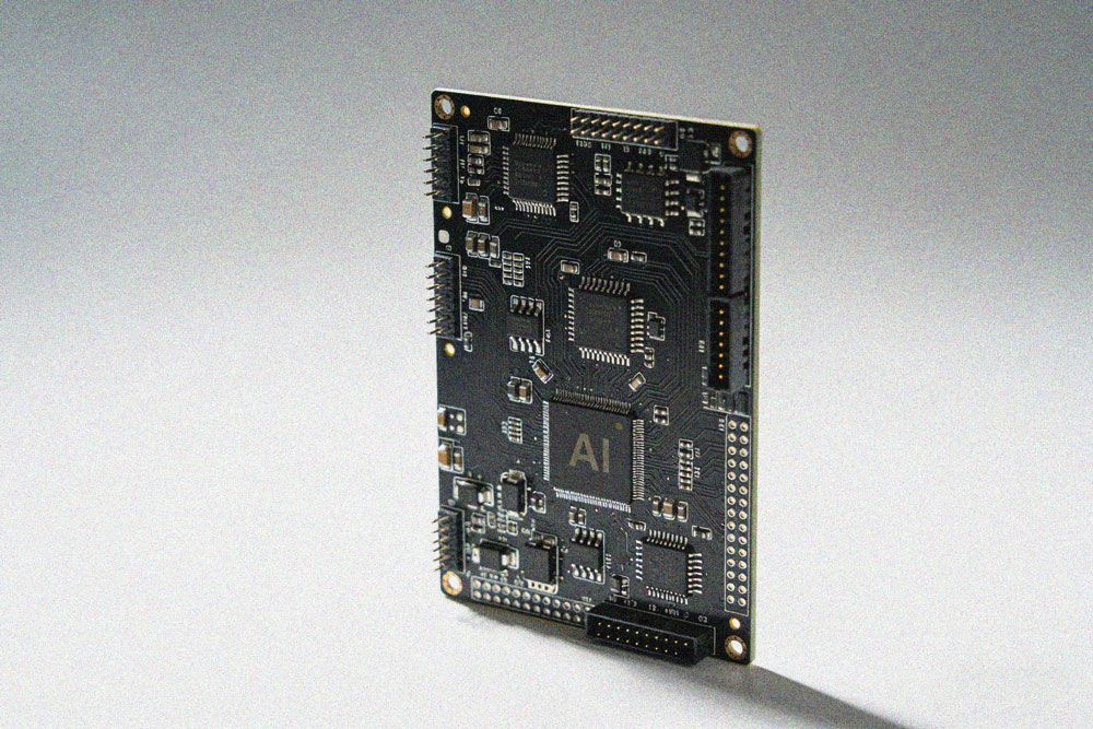
Our technical documentation shows that a typical AI computing server motherboard-like high-multilayer PCB already possesses these characteristics: Utilizing high-speed materials such as TU933+, with 16 to 32 layers, and a minimum aperture of 0.2mm. These parameters directly support high-speed interconnects between High Bandwidth Memory (HBM) and the GPU, as well as between the GPU and external PCIe and network interfaces. Our design capabilities demonstrate that signal transmission rates can reach 112Gbps in the prototype stage, providing a hardware foundation for cutting-edge applications such as 800G optical modules.
High-Density Interconnect (HDI) and Substrate-Like PCB (SLP) Technologies Become Standard
Chiplet architecture brings more interconnect points. To accommodate these high-speed differential pairs and massive power networks within a limited space, PCBs must evolve towards higher densities. This drives HDI (High-Density Interconnect) and Substrate-Like PCB (SLP) technologies from optional to mandatory.
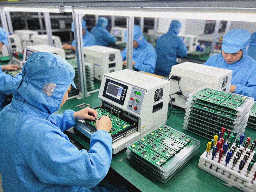
Our process capabilities show that HDI boards can achieve 30 layers of arbitrary interconnects in the prototype stage. For IC carrier boards, the minimum linewidth/spacing can reach 25/25μm (prototype). In specific products, such as the AI accelerator card HDI board, a two-tiered via stacking design with mechanical blind vias is employed, along with BGA laser-filled vias and resin pad-in-hole technology to address reliable connectivity issues in high-density BGA areas.
For FC-CSP packaging substrates, which more closely resemble chip packaging requirements, the process is even more refined: a 6-layer structure, only 0.35mm thick, with linewidth and spacing requirements ≥25/50μm. This "carrier-like" technology, situated between traditional PCBs and packaging substrates, is key to achieving efficient, short-distance interconnection between multi-chip modules and the motherboard.
Signal Integrity (SI) and Power Integrity (PI) Designs Are Unprecedentedly Complex
As data rates approach 112Gbps and multiple computing units with power consumption potentially reaching hundreds of watts are integrated on the board, the challenges of SI and PI are compounded. Each channel's losses, reflections, and crosstalk must be precisely controlled, while ensuring that power network voltage fluctuations are sufficiently small during instantaneous load changes.
Our design services include specialized SI signal integrity analysis and simulation capabilities, providing simulation optimization for DDR4/5 and 2.5-100G high-speed serial channels, and performing power IR-Drop and PDN impedance analysis. In real-world examples, such as designing a motherboard for a network security platform with a CPU power requirement of 130A, we addressed this by planning two 2oz power layers. For high-speed signals, we optimized the layout, allowing surface-level traces to directly enter the PCIe slot, reducing stubs and layer-swapping vias to improve signal quality.
In the edge AI computing evaluation board project based on the NVIDIA Jetson AGX Xavier, we encountered typical high-speed and high-power challenges. This board employs a 10-layer design, meticulously calculating the stack-up structure to strictly control the characteristic impedance of critical differential lines to 100Ω, and features four complete ground planes to provide a low-impedance return path for high-speed signals. Simultaneously, an independent power monitoring and management module is integrated to balance power supply and reduce noise in real time.
Thermal Management From "Heat Dissipation" to "Thermal Design"
CoWoS packaging tightly arranges multiple high-power chips, resulting in extremely high heat flux density. The PCB is no longer merely a passive conductor of heat but needs to actively participate in system thermal planning. This requires thermal management to be a core constraint from the initial design stage.
Our product line includes board types specifically designed to address high heat dissipation requirements, such as thermoelectrically separated copper substrates and high-heat-dissipation aluminum substrates. In AI hardware scenarios, in addition to selecting high thermal conductivity materials, it is crucial to consider heat dissipation paths collaboratively during the PCB layout stage. For example, in the Jetson evaluation board design, we placed high-power chips in locations conducive to airflow and reserved space for heatsink installation. In server motherboard design, even special horizontal layouts of DIMM memory are required to ensure proper airflow.
Advanced Processes and Materials Drive Reliability Improvements
hardware often operates 24/7 in harsh environments such as data centers, demanding extremely high reliability. The high density brought by advanced packaging, in turn, relies on more advanced PCB manufacturing processes to achieve reliability.
Our manufacturing capabilities cover a range of specialized processes supporting advanced packaging: multiple back-drilling, resin-filled vias, through-pads, hybrid surface treatments, and rigid-flex bonding. For example, in AI server motherboard products, we utilize precision control technology for metallized slots, as well as multiple back-drilling and high-density resin-filled via technology, to ensure the mechanical stability and signal integrity of high-speed connectors.
Regarding materials, for high-temperature and high-humidity environments, we use high-Tg materials (e.g., Tg≥170℃). In AI edge devices that need to withstand outdoor or industrial environments (such as smart agricultural controllers), we use immersion gold coating to enhance corrosion resistance and conformal coating to provide additional protection for the PCBA. Conclusion: Collaborative Innovation Through Integrated Design and Manufacturing
PCB advanced packaging design driven by Chiplet and CoWoS technologies is a comprehensive engineering project encompassing ultra-high-density interconnects, ultimate signal and power integrity, system-level thermal management, and cutting-edge materials processes. It blurs the lines between PCB design, manufacturing, and chip packaging.
Faced with these trends, simple design or manufacturing capabilities are no longer sufficient. It requires service providers to possess full-chain closed-loop capabilities, from chip selection and system architecture design (IPD) to high-precision PCB manufacturing and integrated assembly and testing (IPM). We utilize our self-developed EDA tools (such as KBEDA SKILL, which has over 400 manufacturability design checks) to perform pre-manufacturability optimization at the design stage, and then transform this highly complex design into a reliable product through flexible manufacturing capabilities covering from prototype to mass production (without minimum order quantity restrictions). For example, we can provide a one-stop solution for AI computing PCB design, from high-speed simulation and high-density layout to manufacturing using special processes such as arbitrary-level HDI and thick copper blind/buried vias.
The race in AI computing is not only a race of chips, but also a race of its supporting platform—advanced PCBs. Only companies that deeply understand chip packaging trends and achieve collaborative innovation in PCB design and manufacturing can help customers deploy cutting-edge AI computing power stably and efficiently in real-world applications.
Designing AI PCBs for Chiplet and CoWoS Architectures?
- HDI / SLP feasibility review
- SI/PI co-simulation
- Thermal-aware stack-up design
- Prototype-to-production support