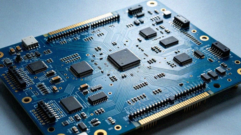
Against the background of rapid iteration of artificial intelligence technology, humanoid robots and intelligent automation equipment are becoming the core focus of the manufacturing industry. As the "nerve center" of the robot, the Joint Control Module puts forward extreme requirements for the integration and signal integrity of the circuit board. AI Robot HDI PCB Design is no longer just a carrier of electrical connections, but also a key physical basis that determines motion control accuracy and response speed. With the deepening of the application of high-density interconnect technology in limited spaces, how to achieve stable transmission of fine lines in multi-layer structures has become a major technical challenge faced by HDI PCB manufacturers.
Core pain point: The game between limited space and signal integrity
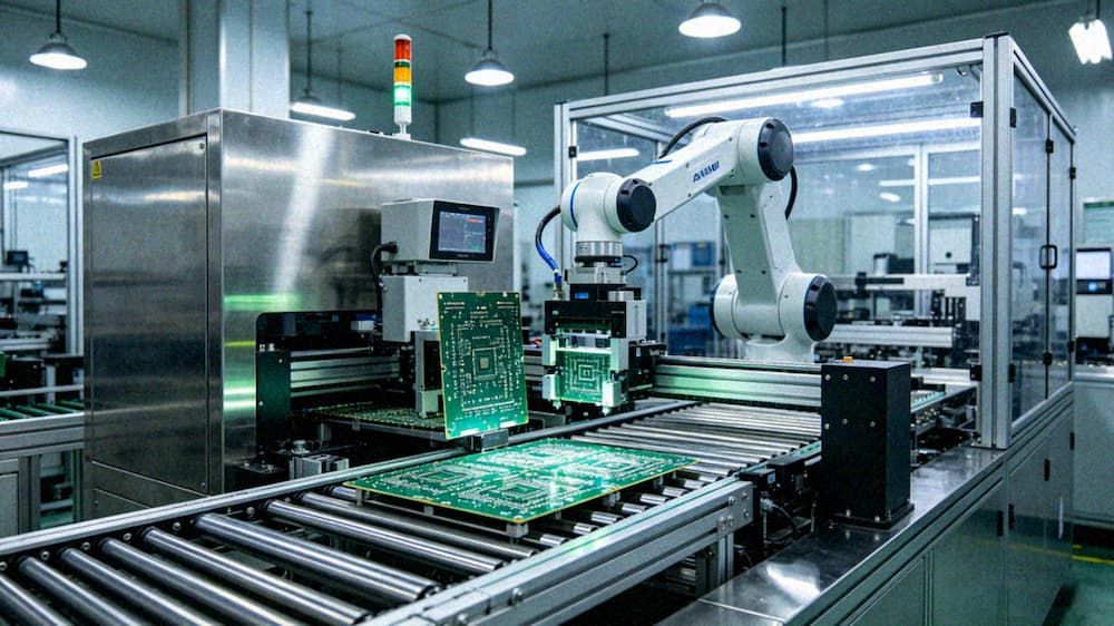
In the physical architecture of the joint control module, the PCB needs to accommodate the main control chip, drive circuit and sensor interface in a very small volume. The traditional multi-layer board process is difficult to meet the wiring density requirements of ai robot hdi pcb, especially in high computing power scenarios involving AI computing PCB design, signal crosstalk and impedance discontinuity will cause control instruction delays. In addition, the continuous movement of robot joints requires circuit boards to have extremely high mechanical reliability, and conventional processes are prone to interconnect failure in a vibration environment. For AI sensor PCB manufacturers, solving micro-hole filling quality and inter-layer alignment accuracy is the core pain point to improve yield.
Technical solution: High-end HDI and material selection optimization
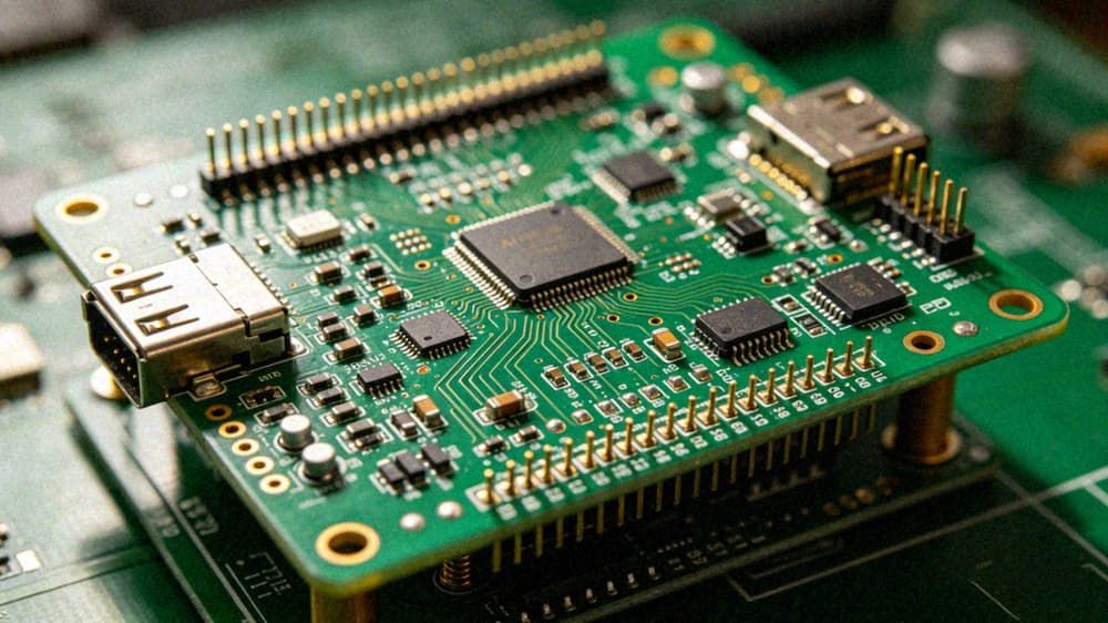
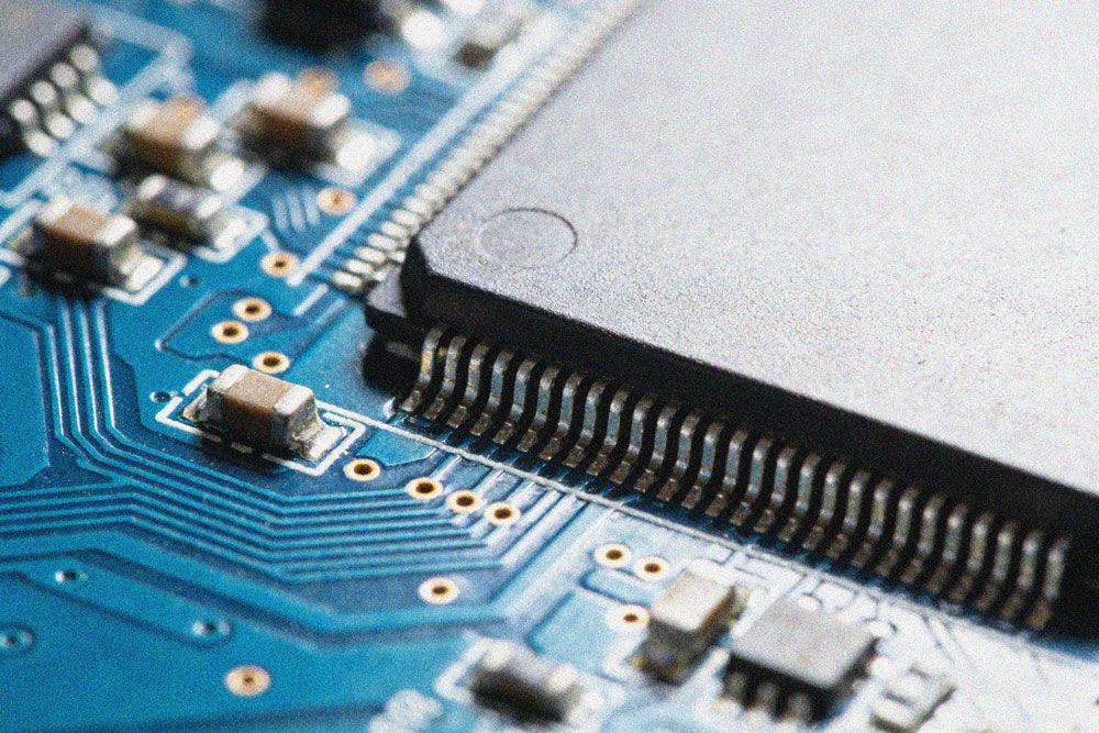
In response to the above challenges, based on the best practices of HDI PCB Design, the use of high-order stacked via structures has become an inevitable choice. According to process capability data, the HDI staggered hole structure can support 10-14-level layer design, and the line width and line spacing accuracy reaches 0.075/0.075mm, significantly improving the wiring density. In terms of substrate selection, high-speed halogen-free materials or high-performance boards such as TU933+ and Panasonic M6 are widely used to ensure low-loss characteristics of signals under high-frequency transmission. For the AI server PCB manufacturers reference solution that requires a higher number of layers, the high multilayer board process of 16-32 layers also provides expansion possibilities. The minimum aperture is controlled at 0.2mm, and the distance from the inner layer hole to the line is ≥7mil, which meets the isolation requirements of complex power and signal networks.
In terms of impedance control, high-precision impedance control technology maintains tolerances within ±8%, effectively ensuring the quality of high-speed signals. The surface treatment process adopts an immersion gold + segmented gold finger solution. The thickness of the gold finger is controlled at 15-30 micro inches, which not only ensures contact reliability, but also adapts to the rapid verification needs of the PCB Prototype stage. This process combination is not only suitable for mass production of PCB Fabrication, but also provides process redundancy for the miniaturized design of ai robot sensor module pcb.
Case verification: humanoid robot main control and drive system
At the practical application level, the head core control system of a humanoid robot project provides a typical example. The core board adopts a car-grade design and a composite heat dissipation system, and uses STM32H7 as the core main control chip. The MCU uses a three-power domain architecture and can develop flexible low-power solutions. In the design of the joint driver board, a specialized motor driver chip MagnTek-MT6835GT is used to provide sufficient current and voltage to drive motors of different types and powers.
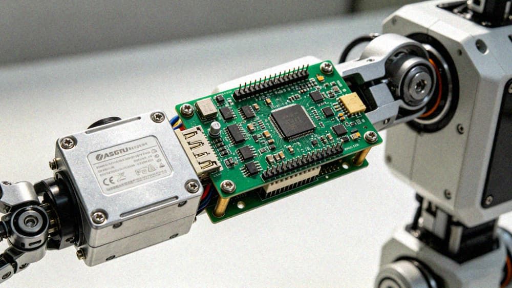
In addition, the infrared camera control system case shows that the core board uses RV1126K as a high-performance AI vision processing chip, supporting 4K@30fps high-definition video encoding and decoding. The base material is S1000H, the plate thickness is set to 1.6mm, and it adopts a 6-layer structure design with a copper thickness of 1oZ to meet the strict requirements of current carrying capacity and signal transmission. Through the introduction of high-density interconnection technology, the circuit layout can be precise and the power supply and control functions can be efficiently integrated. This design idea is also applicable to intelligent lawn mowing robot and industrial robot arm main control board, reflecting the versatility and adaptability of HDI PCB technology in multiple scenarios.
Conclusion and Outlook
To sum up, the successful implementation of AI robot HDI PCB design relies on the systematic collaboration of materials, structures and processes. From 0.075mm fine lines to 10-14-step stacked hole structures, the optimization of every parameter is directly related to the performance of the final product. With the further integration of AI sensor PCB manufacturers and HDI PCB manufacturer technologies, future joint control modules will evolve towards higher integration and lower latency. Through one-stop integrated design and manufacturing (IPDM) solutions, a full-chain closed-loop system from design to manufacturing will be built, thereby promoting the intelligent leap forward of joint control modules and even the entire robot industry.