Yes. Our PCB design services offer scalable solutions for prototype PCB assembly and high-volume PCB manufacturing, ensuring quality and efficiency at every stage of production.
View More >>Microelectronics Bonding Equipment
Microelectronics Bonding Equipment
Microelectronics Bonding Equipment 1
Microelectronics Bonding Equipment 2
Microelectronics Bonding Equipment 3
Microelectronics Bonding Equipment 4
Overview
Microelectronics Bonding Equipment (PCB Solution) | Semiconductor Core Packaging
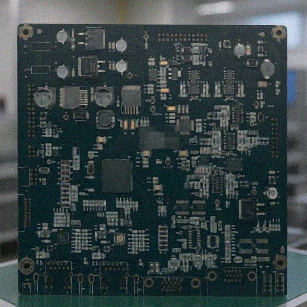
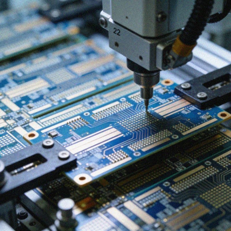
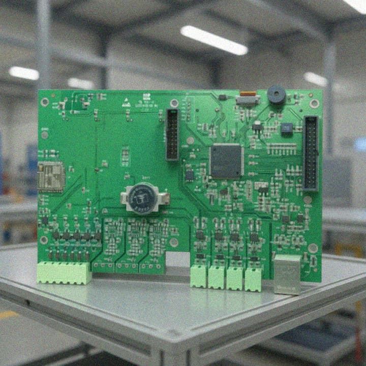
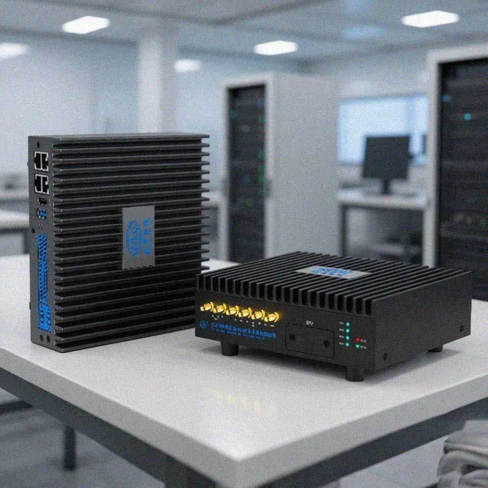
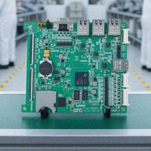
In the industrial robotics sector, the customer required a high-precision multi-layer HDI bonding control PCB. The board specifications included inner-layer line width ≥2 mil, inner-layer spacing ≥2 mil, outer-layer spacing ≥2.5 mil, and a total of 22 layers, with extremely tight via alignment requirements, making production highly challenging.
We employed multiple laser via alignment processes, high-precision multi-layer lamination, and BGA laser-filled vias combined with resin-in-pad plating to achieve accurate HDI structures.
As a result, soldering pass rates were significantly improved, the project progressed efficiently, and debugging and rework time were greatly reduced, lowering rework, maintenance, and scrap costs.
| Category | Details |
|---|---|
| Project Name | Microelectronics Bonding Equipment (PCB Solution) | Semiconductor Core Packaging |
| Customer Sector | Industrial robotics |
| PCB Requirements | - High-precision multi-layer HDI bonding control PCB - Inner-layer line width ≥ 2 mil - Inner-layer spacing ≥ 2 mil - Outer-layer spacing ≥ 2.5 mil - Total layers: 22 - Extremely tight via alignment requirements |
| Manufacturing Processes | - Multiple laser via alignment processes - High-precision multi-layer lamination - BGA laser-filled vias with resin-in-pad plating |
| Outcomes | - Significantly improved soldering pass rates - Efficient project progression - Greatly reduced debugging and rework time - Lowered costs related to rework, maintenance, and scrap |
Share To:
Our faqs
Frequently Asked Questions.
- Can your EMS services handle both prototype and large-scale PCB production?
- Do you assist with PCB layout and design optimization?
Yes. We specialize in PCB design and layout services and incorporate design for manufacturing(DFM) principles to optimize layouts, reduce costs, and improve production workflows, ensuring that your PCB project runs smoothly and efficiently.
View More >> - Do you offer BOM services for EMS manufacturing?
Yes. We provide complete Bill of Materials (BOM) service support, including material selectionand sourcing, to streamline your production process and enhance EMS manufacturing efficiency.
View More >> - How do you ensure quality in PCB manufacturing?
To guarantee our reliability and performance, we rigorously employ advanced techniques in ourPCB design services, adhering to international standards and performing rigorous electronicengineering and testing. We are certified with ISO 9001, ISO 50001, ISO 45001, ISO 14001, ISO 13485, IATF 16949, ROHS, UL, COC and AEO. Whether it is a flexible PCB, multilayer, HDl, metal board, rigid-flex, or optical communication PCBmanufacture, we ensure every product meets the highest quality benchmarks.
View More >> - What about our PCB production equipment?
We possess advanced production equipment in key processes, ensuring that product precision and consistency meet the optimal state required by the market demands. For instance, all inner and outer layer circuits are produced using LDI, and we have the most advanced Mitsubishi laser drilling machines and laser blind hole copper filling VCP for creating mechanical
View More >> - What files are required for a PCB manufacturing quote?
Gerber files, PCB specifications, and your target quantity.
View More >>
Related Solutions
More Solutions in This Category


ABOUT OUR COMPANY
Hardware Solution and Manufacturing Service Provider
Founded in 1997 and headquartered in Shenzhen, KINGBROTHER specializes in electronic interconnection technologies and hardware innovation. We focus on electronic product R&D, AI hardware solutions, engineering services, integrated design and manufacturing, and supply chain capabilities to deliver comprehensive PCB manufacturing, IPD (Integrated Product Development), and EMS services.
We are committed to becoming a world-class AI hardware solutions and manufacturing service provider, offering one-stop solutions for AI robots, industrial control, medical devices, new energy, and automotive electronics, helping our customers accelerate innovation and bring products to market faster.
We bridge R&D to mass production with integrated capabilities:
Precision-Driven System Design to Accelerate Your Success
We adhere to systematic design as our foundation, offering hardware, software, and industrial design services. With 6 self-owned design centers and a knowledge base including 3.27 million certified materials and 2,368 DFI rules, we significantly reduce design iterations by 60-80% and increase customer project success rates by 35%.

End-to-End Technical Integration for Unbroken Innovation
We have built an integrated technology chain from IC design IPD and PCB to integrated product manufacturing IPI. With 300+ technical solutions and over 2,500,000 product models and project verifications, we achieve closed-loop collaboration and optimization throughout the hardware innovation process.

Rigorous Engineering for Uncompromising Product Integrity
Through strict QIS quality management systems and full-chain engineering empowerment via DF8, failure analysis, and process control, we eliminate 90% of pad defects and 70% of assembly risks, ensuring product safety for our customers.

Agile Manufacturing and Supply Chain for On-Demand Fulfillment
Leveraging 5 IPI smart manufacturing bases and a cloud alliance of over 100 factories, we have established a flexible production system for small-batch, multi-batch needs. Our mature global supply chain ensures quick response and delivery, especially in component procurement.

Services
We provide services to 20,000+ clients
The Choice of Dozens of Fortune 500 Companies.

PCB Manufacturing Service
With 29 years of expertise in high-end and specialty PCBs, we deliver reliable and flexible manufacturing solutions. We offer prototyping, quick-turn, and small-to-medium volume PCBs, including multilayer, HDI, high-copper, and rigid-flex boards, backed by a one-stop PCB service that empowers clients across industries, from AI hardware to cutting-edge electronics, to accelerate product innovation and bring ideas to market faster.

Electronic Manufacturing Service
Reliable AI hardware solutions with full-lifecycle supply chain support. We provide highly reliable electronic manufacturing services. Our integrated PCBA, BOM management, NPI engineering and advanced failure analysis to guarantee reliable performance at every stage.

Electronic Product Design Service
We focus on independent design house (IDH) and CAD design, providing AI hardware solutions and covering services such as hardware design, software design, industrial design, and EDA development.
Our Solutions
Full-Stack Electronics Solutions
100% Complete & Professional Solutions: From Design to Manufacturing.


Contact us