With the large-scale implementation of the new energy industry, energy storage systems have become the core hub for achieving "source-grid-load-storage" synergy in the energy internet. Their intelligence level and operational reliability directly determine energy utilization efficiency. Printed circuit boards (PCB), as the core physical carrier of energy management modules and AI computing units in energy storage systems, require sophisticated design and manufacturing; this is a crucial foundation for the implementation of smart energy AI systems. Under the Integrated Product Design and Manufacture (IPDM) technology system, precise design of the Energy storage AI server PCB and the professional manufacturing capabilities of Energy management PCB manufacturers are becoming core supports for energy storage systems to overcome performance bottlenecks and achieve efficient operation.
KingBrother IPDM One-Stop Integrated Design & Manufacturing
Through full-chain technology integration, KingBrother delivers end-to-end one-stop services from product design to integrated manufacturing, covering three core business segments: Integrated Product Design (IPD), Integrated Product Manufacturing (IPM), and Printed Circuit Board (PCB).
Integrated Product Design (IPD)
Reliable Design Capability With 6 major design centers, we bring together hundreds of outstanding domestic and international designers with years of accumulated development experience. Our design services cover all critical links from complete product development to manufacturing implementation.
In-Depth Technical Support We maintain in-depth cooperation with the world's leading chip original manufacturers, providing full-spectrum technical support from underlying hardware to software systems.
Systematic Assurance Capability We provide full-process systematic management, backed by a structured, asynchronous and platform-based development workflow.
Self-Developed EDA Auxiliary Tools KBEDA SKILL, a secondary development tool based on the Cadence software platform, is equipped with more than 400 application functions. A number of these functions have been granted software copyrights and patent authorizations, which effectively help improve design quality and shorten R&D cycles.
Integrated Product Manufacturing (IPM)
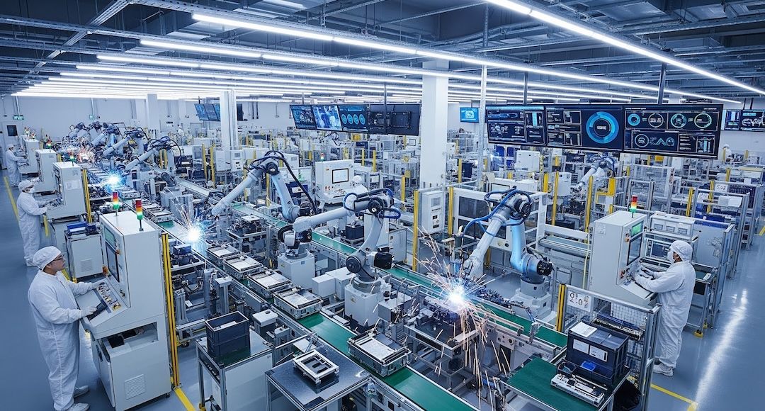
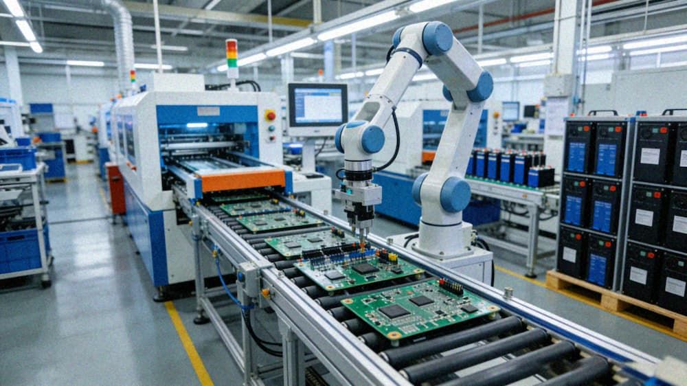
Accelerated R&D Prototyping We provide one-stop integrated design and manufacturing solutions, covering full-process services from component procurement, PCBA (Printed Circuit Board Assembly) to engineering testing. Our efficient BOM supply chain platform ensures stable supply and controllable costs, with partnerships with over 2,000 global brands and agents and tens of millions of industry BOM data entries.
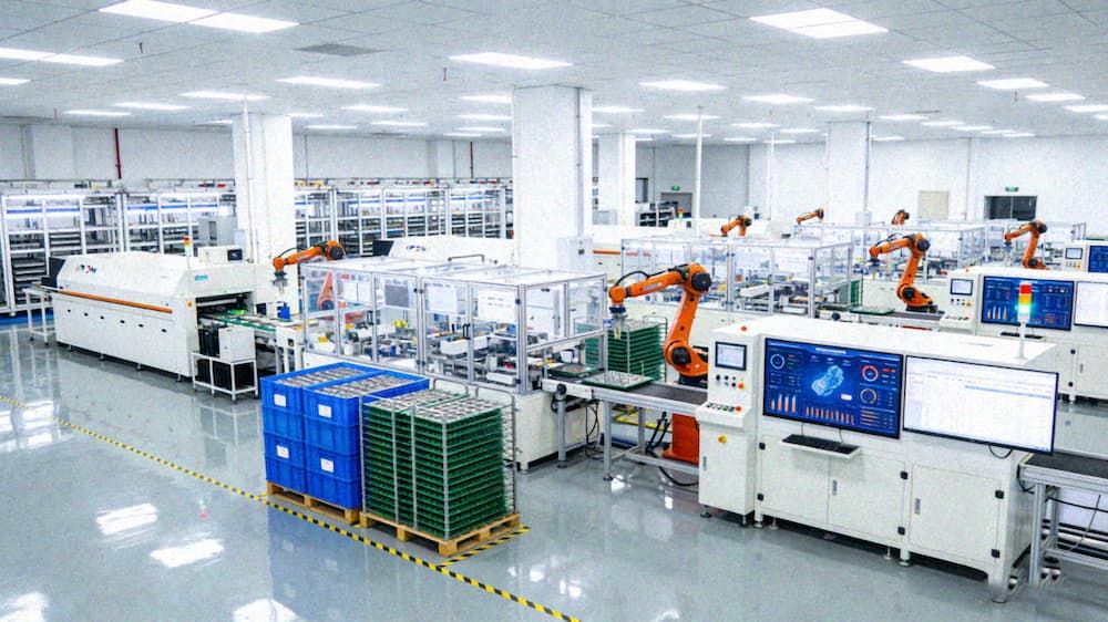
One-Stop Service Capability for Batch Supply Assurance Supported by 5 major EMS (Electronics Manufacturing Services) manufacturing bases and more than 20 advanced production lines, we provide 7×24 rapid response services.
Printed Circuit Board (PCB)
Flexible Manufacturing System With 2 major PCB manufacturing bases, we have built a R&D service-oriented flexible production system.
Rapid Delivery Capability We offer expedited prototyping services with a minimum lead time of 24 hours, supported by 7×24 full-process operation, to flexibly meet the demands of R&D iteration and multi-batch, small-volume orders.
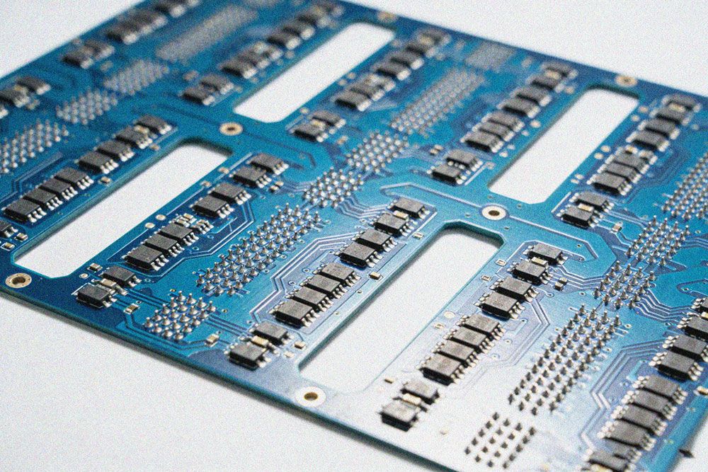
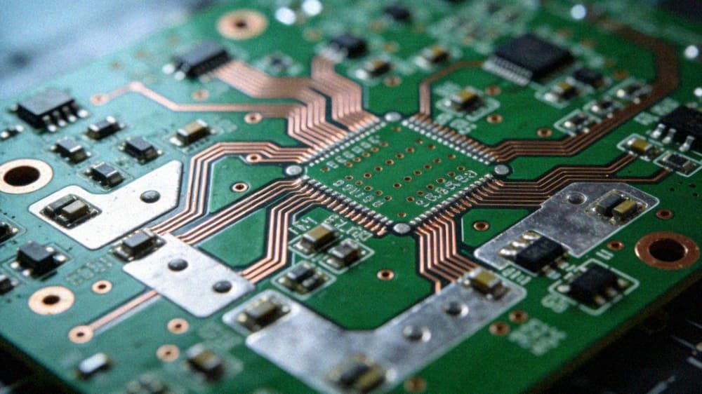
Full Product Category Coverage Our product portfolio covers high-frequency & high-speed boards, rigid-flex boards, HDI (High-Density Interconnect) boards, high thermal conductivity boards, embedded boards, and package substrates, fully meeting the needs of customers across various industries. Our process capabilities cover 72-layer FR4 boards, any-layer HDI products and more.
High Product Reliability We have passed stringent system certifications including ISO9001 and IATF16949 (for automotive electronics). Our CNAS/CMA accredited Zhilian Testing Center provides professional and comprehensive testing capabilities.
Core of IPDM Practice: Underlying Requirements of Energy Storage AI Systems for PCB
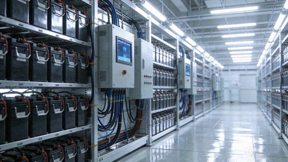
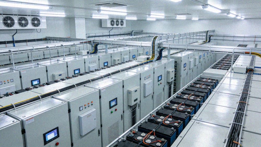
IPDM is not a traditional power distribution component, nor a single hardware module, but a systematic engineering philosophy and technology system of Integrated Product Design and Manufacture, which focuses on the deep synergy of product design, process manufacturing and system application requirements throughout the product lifecycle; its practice runs through the whole chain of R&D, production and application of core hardware for smart energy AI systems. As the core hardware carrier practicing IPDM (Integrated Product Design and Manufacture), the Energy Storage AI Server PCB must simultaneously meet two major requirements: first, it must adapt to the high-performance data transmission requirements of AI servers; second, it must withstand the harsh operating environment of energy storage scenarios, characterized by high voltage, high current, wide temperature range, and strong electromagnetic interference.
According to an industry report released by the China Electronic Components Industry Association in 2024, the domestic market size for PCBs used in energy storage grew by over 45% year-on-year, with Energy Storage AI Server PCBs, designed for AI computing power scheduling, accounting for 28% of the market. This data confirms the core value of this type of PCB in energy storage systems. Within the IPDM (Integrated Product Design and Manufacture) framework, efficient PCB design must revolve around integrated characteristics: On one hand, multi-layer board architectures optimize signal transmission paths, and power layer partitioning is implemented for the computing modules of energy storage AI servers to control ripple interference within ±5mV, ensuring stable operation of AI algorithms. On the other hand, AI simulation technology is integrated to perform comprehensive verification of PCB layout, anticipating thermal and electromagnetic compatibility (EMC) issues in advance. For example, thermal simulation algorithms optimize the layout of heat dissipation pads, reducing PCB operating temperature by 8-10℃, adapting to the enclosed operating environment of energy storage power stations.
The large-scale application of energy storage systems places triple demands on energy management PCB manufacturers: high precision, high reliability, and high production capacity. Their manufacturing capabilities directly determine the landing effect of IPDM philosophy and technology system.
In terms of raw material control, leading energy management PCB manufacturers have established a rigorous supplier certification system. PCBs used in energy storage employ high Tg (≥170℃) copper-clad laminates, combined with halogen-free flame-retardant resin materials, meeting the wide temperature range operation requirements of -40℃ to 85℃ in energy storage scenarios. They also comply with the UL94 V-0 flame-retardant standard, reducing safety risks from the source.
At the process technology level, for the high-density packaging requirements of PCBs under the IPDM system, mainstream manufacturers have widely adopted laser direct imaging (LDI) technology, controlling line tolerances within ±20μm. This represents a 50% improvement in accuracy compared to traditional exposure processes and can accommodate the soldering of micro-pitch devices with a 0.2mm pitch. Simultaneously, vacuum lamination technology replaces traditional lamination methods, increasing interlayer bonding strength by 30%, effectively reducing the risk of PCB delamination and cracking during long-term operation of energy storage systems. Furthermore, a comprehensive quality inspection system has become standard practice—AOI (Automated Optical Inspection) covers circuit fabrication and solder mask printing, X-ray inspection verifies the soldering quality of BGA packaged devices, and electrical performance testing before shipment ensures that the conduction resistance, insulation resistance, and other indicators of each PCB meet the design and application standards under the IPDM technical system.
Industry Value and Trends of IPDM Practice
The IPDM practice in smart energy AI systems, through the efficient design of Energy storage AI server PCBs and the precise manufacturing by Energy management PCB manufacturers, has improved the synergistic efficiency of "computing power-energy" in energy storage systems. Taking a megawatt-level energy storage power station application case as an example, after adopting a PCB solution optimized based on IPDM, the response latency of the AI energy dispatch module decreased from 200ms to 170ms, the overall system energy efficiency improved by 8%, and the annual power generation increased by approximately 120,000 kWh, validating the commercial value of this practice.
In the future, as energy storage systems evolve towards "intelligence, integration, and miniaturization," the design of Energy Storage AI Server PCBs will deeply integrate digital twin technology. By constructing a digital model of the entire PCB lifecycle, it will achieve full-process digital control of design, manufacturing, and operation and maintenance. Meanwhile, Energy Management PCB manufacturers will transform towards "flexible manufacturing and customized production," relying on digital transformation of production lines to quickly adapt to the differentiated needs of products under the IPDM technical system in different scenarios, such as miniaturized PCBs for residential energy storage and high-power PCBs for grid-scale energy storage. Simultaneously, the industry is accelerating the improvement of the energy storage PCB standard system, promoting the coordinated upgrading of design specifications and manufacturing processes, and further improving the reliability and large-scale deployment efficiency of smart energy AI systems.
In summary, the IPDM practice of smart energy AI systems essentially involves precisely upgrading PCB design and manufacturing to connect the core links of energy storage systems: "hardware carrier - energy management - intelligent scheduling." Against the backdrop of the rapid development of the new energy industry, focusing on the design optimization of energy storage AI server PCBs and empowering the manufacturing upgrade of energy management PCB manufacturers will continuously drive the evolution of energy storage systems towards higher efficiency and higher reliability, laying a solid hardware foundation for the construction of smart energy systems.