High-Frequency PCB
Product Overview
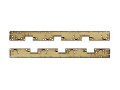
High-frequency PCBs are built using specialized RF materials that offer low dielectric loss and excellent signal stability, enabling reliable high-speed and high-frequency transmission. The design incorporates multiple blind/buried vias for higher routing density, along with multi-step cavity structures that enhance electromagnetic performance and thermal management. This precise, high-integrity architecture makes high-frequency PCBs ideal for applications requiring stringent RF performance. They are widely used in telecommunications, millimeter-wave radar, and advanced radar systems for autonomous driving, providing robust support for high-speed signal processing and RF modules.
| Item | Specification |
|---|---|
| Application | Communication |
| Layer/thickness | 5L/1.9mm |
| Surface finish | Immersion gold |
| Line width/space | 9.0/9.2mil |
| Min hole diameter | 0.3mm |
| Technical features | Three-step groove structure |
Share To:
Our Capabilities
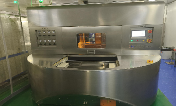
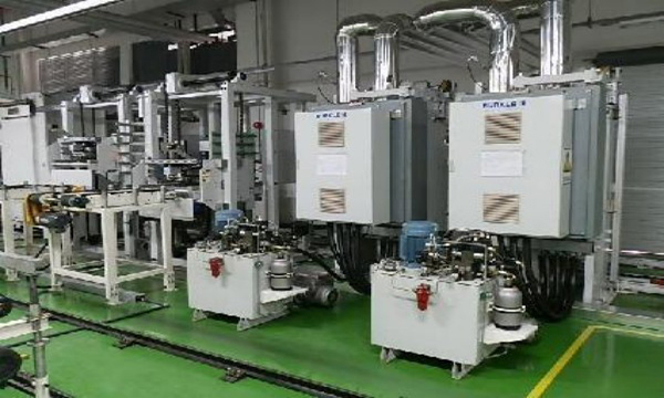
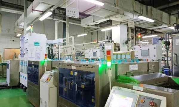
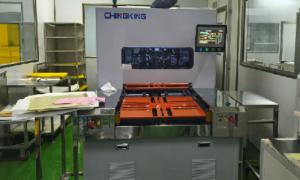
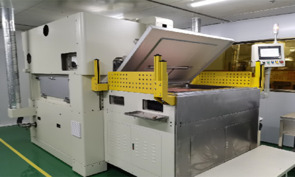
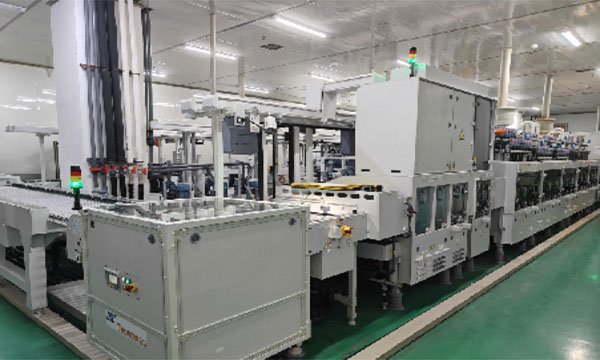
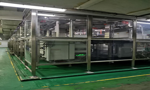
Production Equipment
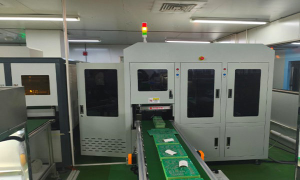
AVI visual inspection machine
Boke Precision Vacuum Laminator
Ceramic grinding machine
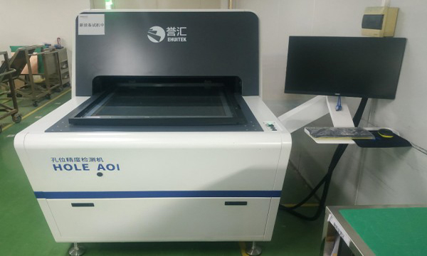
Hole position accuracy testing machine
Lamination hot melt machine
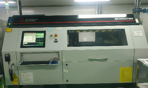
Mitsubishi 6th Generation Laser Drilling Machine
Vacuum Resin Plug Machine
Vacuum two-fluid etching machine
VCP continuous electroplating line