Overview
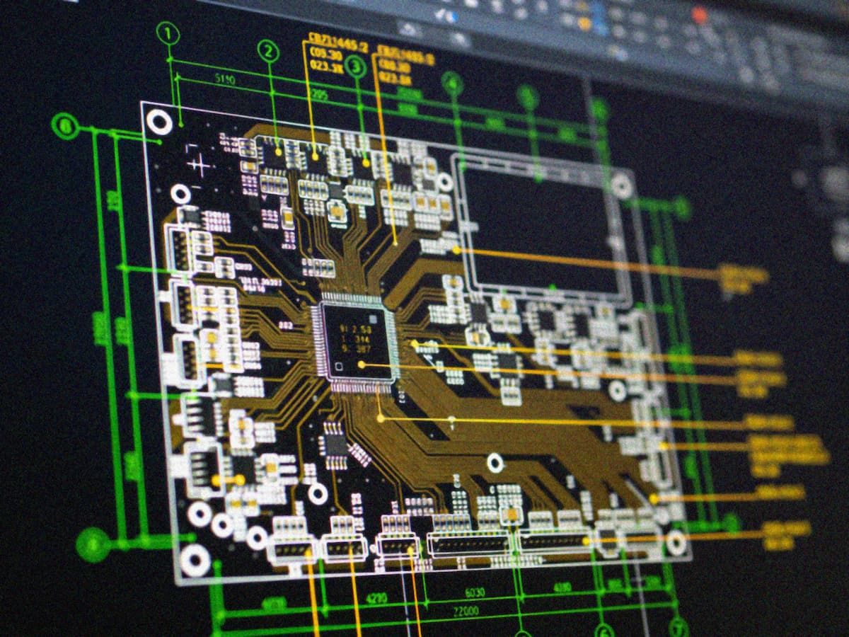
High-speed PCB design is a core technical link for the development of modern high-performance electronic products, targeting the signal integrity, power integrity and electromagnetic compatibility challenges brought by high-frequency, high-bandwidth signal transmission. As electronic products continue to evolve towards higher computing power, lower latency and smaller form factors, high-speed signal links with transmission rates of 10Gbps, 25Gbps, even up to 112Gbps are widely used in communication, automotive, computing and industrial fields. These high-speed signals are prone to problems such as attenuation, crosstalk, impedance mismatch, signal reflection and electromagnetic interference during transmission, which will directly lead to increased signal error rate, reduced product performance, or even failure to operate normally. Systematic high-speed PCB design runs through the entire product development cycle, from schematic verification, stack architecture planning, component placement optimization, routing rule formulation, to post-layout simulation verification and DFM (Design for Manufacturing) review. It comprehensively balances product performance, material cost and manufacturing cycle requirements, providing reliable technical support for the stable operation and mass production of high-speed electronic products.
Technical Capabilities
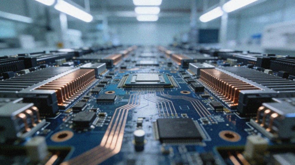
- High-Speed Signal Transmission Support: Supports transmission rates up to 112Gbps for high-speed SERDES links, with universal 25Gbps channel support for common high-speed interface scenarios. The service covers signal integrity simulation for differential pairs, DDR3/DDR4/DDR5 memory interfaces, high-speed optical communication links and other transmission paths, ensuring signal jitter, insertion loss, return loss and other core indicators meet industry standard requirements, minimizing signal loss and error rate across the full transmission path.
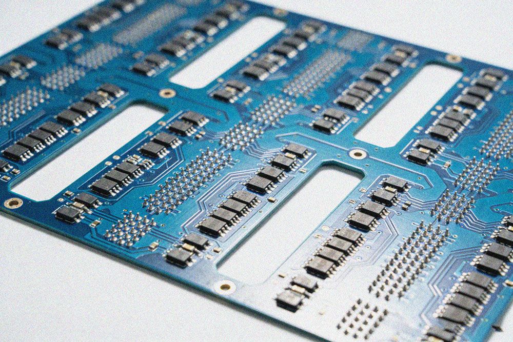
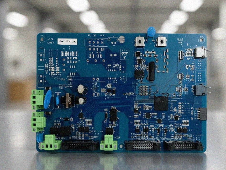
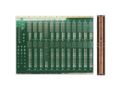
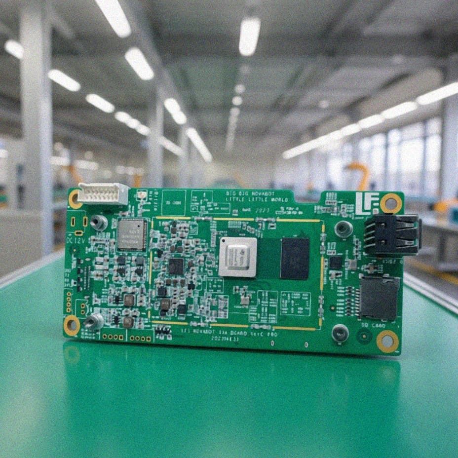
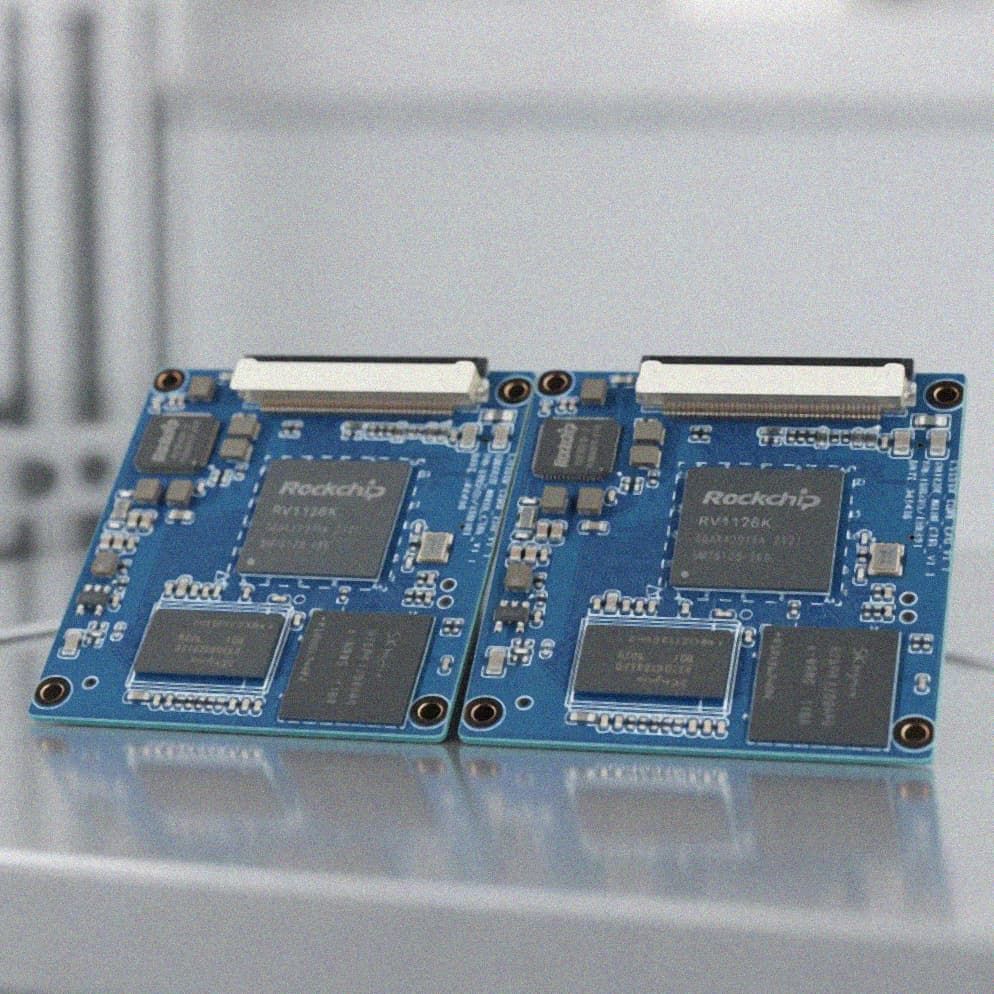
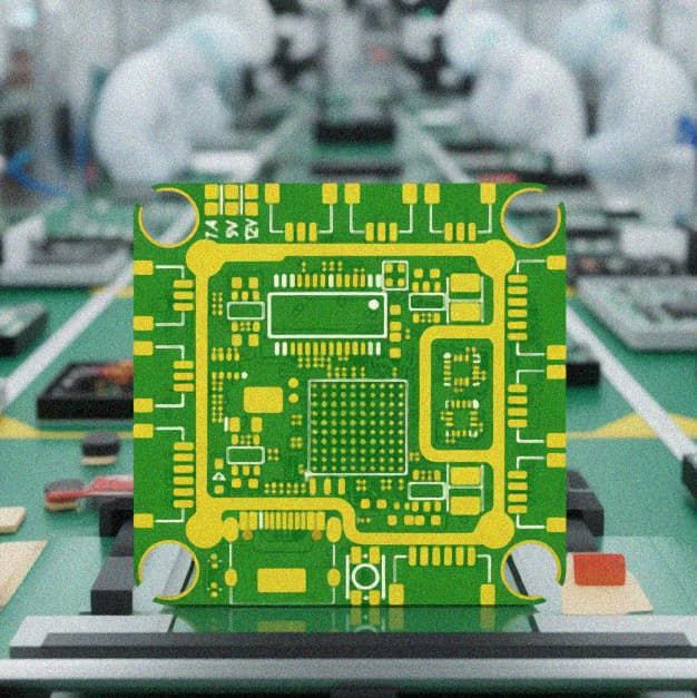
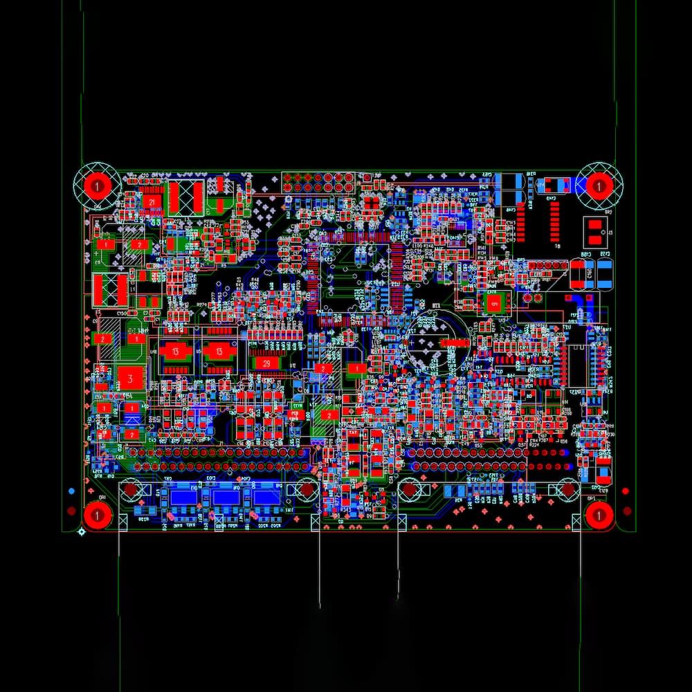
- Multi-Board Type Design Compatibility: Covers design of high-speed, high-density mixed digital-analog PCBs, embedded capacitance resistance boards, HDI boards, rigid-flex boards, high-frequency mixed pressure boards, pure PTFE high-frequency boards, and IC substrate designs. It supports layer counts up to 68 layers for FR4 materials, 30 layers for rigid-flex boards (with up to 12 flexible layers), 28 layers for high-frequency mixed pressure boards, and 28-layer any-step HDI designs, adapting to diverse high-performance product architecture and form factor needs.
- Precision Stack and Impedance Control: Provides customized stack planning based on product signal density, bandwidth and electromagnetic shielding requirements, with configurable independent ground plane solutions to effectively shield inter-layer signal crosstalk. It achieves high-precision impedance control for 90Ω, 100Ω and other common differential and single-ended impedance specifications, with strict error control to reduce signal reflection and transmission distortion, ensuring consistent signal quality across all high-speed links.
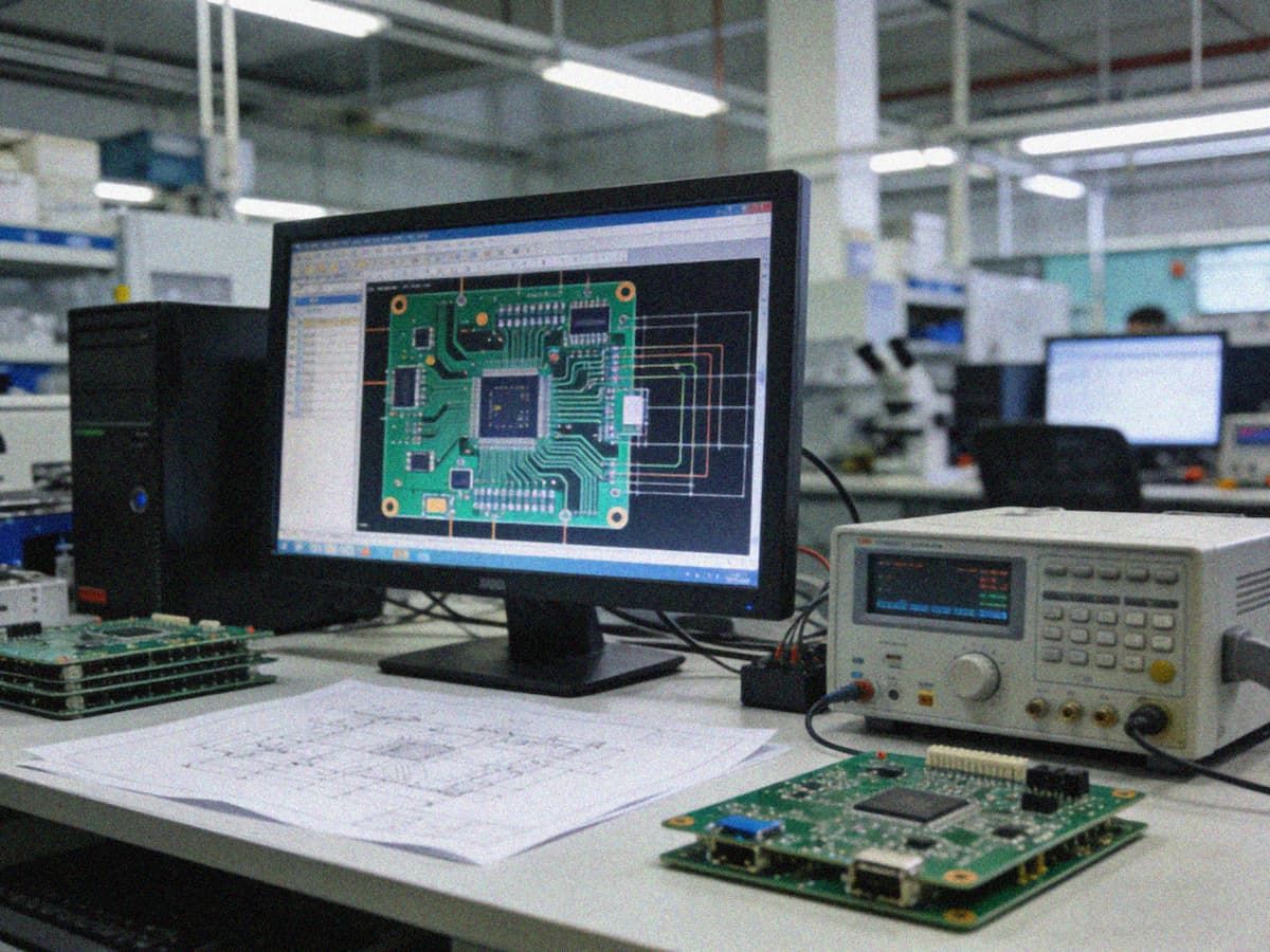
- Full-Process Verification Support: Includes pre-layout signal integrity (SI) analysis, power integrity (PI) analysis, EMC pre-compliance testing, post-layout simulation verification, and multi-dimensional DFM review. The design process identifies potential signal risks, power supply ripple issues, electromagnetic compatibility hazards and manufacturing feasibility problems in advance, avoiding repeated design revision cycles and reducing post-production adjustment costs.
- Diversified Design Service Coverage: Offers full design services from schematic optimization, PCB layout, design revision, to design diagnosis and technical training, supporting both new product development and existing product performance upgrade needs, adapting to project demands of different scales from prototype verification to mass production.
Quality Standards
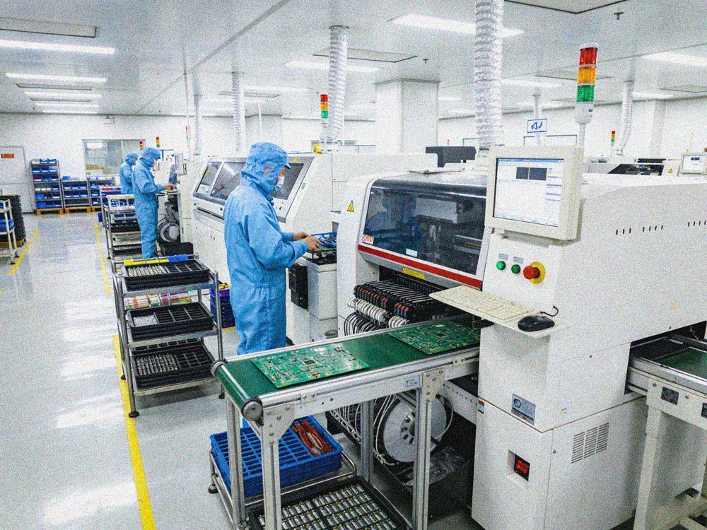
All high-speed PCB design outputs strictly comply with global general industry specifications, including IPC-2221, IPC-2222, IPC-2223 and other standard requirements for rigid, flexible and rigid-flex PCBs, and meet RoHS, REACH and other environmental compliance regulations for different regional markets. Each design stage is equipped with independent review gates, including schematic correctness review, stack architecture feasibility review, component placement rationality review, high-speed routing rule compliance review, simulation verification result review, and DFM manufacturing compatibility review, each with clear pass criteria to ensure design outputs fully meet both performance and manufacturing requirements. All high-speed designs are validated to match mass production process capabilities, ensuring manufacturing yield of over 98% for qualified designs, reducing production scrap and rework costs.
Applications
High-speed PCB design solutions are widely applicable to various high-performance electronic product scenarios, including but not limited to:
- 5G Communication Equipment: High-speed backplanes, 5G couplers, baseband processing boards, RF front-end boards, optical module carrier boards, supporting high-speed signal transmission between communication core units, meeting low latency and high reliability requirements of 5G access and core network equipment.
- Automotive Electronics: Millimeter-wave radar PCBs, autonomous driving domain controller boards, in-vehicle high-speed Ethernet backplanes, smart cockpit core processing boards, ensuring stable signal transmission in complex automotive operating environments with wide temperature ranges, long-term vibration and strong electromagnetic interference.
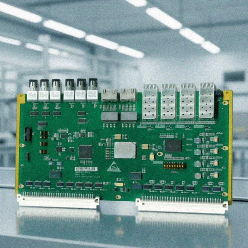
- High-Performance Computing (HPC): Server motherboards, high-speed data exchange switches, storage system control boards, supporting 112Gbps high-speed interconnection between computing units, storage modules and network interfaces, meeting high bandwidth requirements of cloud computing, big data processing and artificial intelligence computing scenarios.
- Consumer Electronics: High-end smart terminal mainboards, AR/VR core processing boards, high-speed data interface expansion boards, adapting to high-density, thin and light design requirements of consumer electronics while ensuring stable high-speed signal transmission for audio, video and large data interaction.
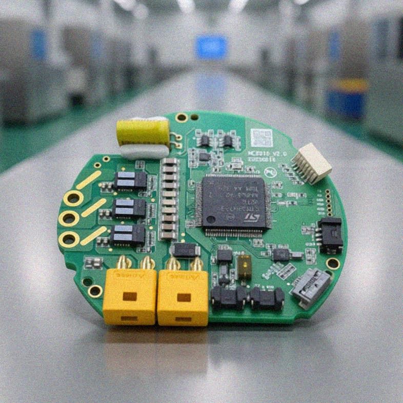
- Industrial Control Equipment: Industrial high-speed communication gateways, industrial vision processing boards, motion control core boards, ensuring long-term stable operation of high-speed signals in harsh industrial environments with dust, high humidity, and wide temperature fluctuations.
Key Advantages
- Performance-Cost-Manufacturing Cycle Optimization: Adopts a systematic design-oriented concept, balancing product signal performance, material cost, and manufacturing cycle requirements at the early design stage, providing the optimal design solution for different project budget and delivery timeline needs, avoiding unnecessary over-design or under-design.
- Rich Industry Standard and Process Experience: Design teams have in-depth mastery of global high-speed PCB manufacturing process standards and industry application requirements, can identify potential manufacturing and application risks in advance during the design phase, reducing subsequent revision and adjustment costs, shortening the product launch cycle.
- Full-Cycle Design Service Support: Covers all links from demand communication, schematic design, layout, simulation verification, prototype testing to mass production guidance, providing one-stop design support to reduce cross-department or cross-vendor communication costs, and ensure consistency between design intent and final product performance.
- Diversified Design Adaptability: Supports customized design for different material systems, board types, and application scenarios, meeting the needs of various high-speed electronic product developments from small-batch prototype verification to large-scale mass production, and providing flexible design revision and optimization services for subsequent product iteration.
Contact Information
If you have high-speed PCB design needs, including new product development, existing design revision, or design performance optimization, you can reach out to our professional technical team at any time. We will provide you with free pre-design consultation, customized design solutions, and full-process technical support to help your high-performance electronic products hit the market efficiently and reliably.