WWDC26 brings on-device AI back into the hardware discussion
Apple has confirmed that WWDC26 runs from June 8 to June 12, with the Keynote and Platforms State of the Union scheduled for June 8. The official agenda points to AI advancements, developer tools, and more than 100 technical sessions. For the consumer electronics supply chain, a software conference like this does not stay entirely in software. Every time platform-level capabilities are opened to developers, part of the workload that once sat in the cloud can shift back toward terminal devices, changing the design limits of main boards, sensor boards, RF modules, and power management circuits.
The hardware implications differ from the AI server PCB discussions that have dominated the past few months. AI server boards are shaped by rack-scale computing, very high layer counts, 112Gbps-class interconnects, and data center power and thermal constraints. WWDC26 points instead toward phones, tablets, wearables, spatial computing devices, and edge AI cameras. For procurement teams, the practical question is whether Apple Intelligence, Siri upgrades, machine learning APIs, and visual intelligence features will bring simultaneous pressure in HDI density, low-power design, EMI control, and NPI cycle time.
That pressure will not arrive as a single specification change. It is more likely to appear through a series of design requests: more sensors sharing a smaller board area, more local inference running under tight battery limits, more high-speed memory traffic near RF front ends, and shorter validation cycles as device brands race to turn software features into hardware experiences. These changes are manageable individually, but they become difficult once they converge inside compact edge devices where layout, thermal paths, shielding, and assembly yield are already constrained.
The PCB difficulty in on-device AI sits in power, memory, and RF coexistence
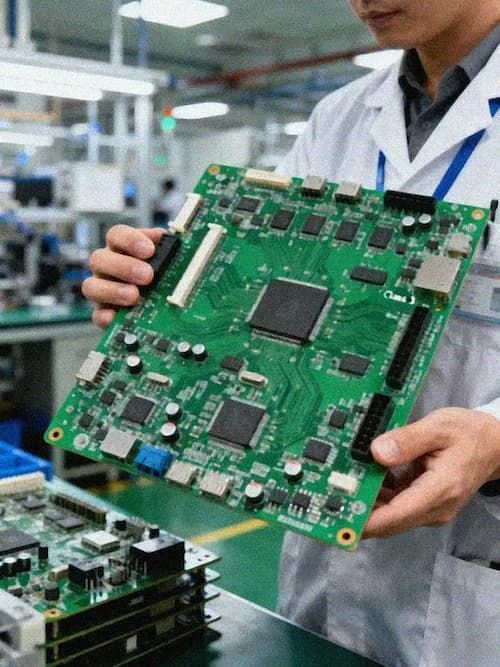
On-device AI depends on local NPU, GPU, ISP, and memory subsystems working together. At the software layer, users see voice assistants, image editing, real-time translation, and personalized recommendations. At the hardware layer, those features translate into higher transient current, denser high-speed memory routing, more sensor inputs, and more frequent wireless activity. For Edge AI Devices, PCB design is no longer just a matter of fitting an AI-capable chip into an existing board outline; it requires a new balance among power integrity, signal integrity, thermal paths, and RF isolation within a tightly constrained area.
A smartphone or AI camera provides a useful example. When the main SoC runs local inference, load transients can become sharper than in ordinary application scenarios, making rail droop and ripple more sensitive. If decoupling capacitors sit too far from the load, or if a power plane is cut by high-speed signal routing, an NPU load step can create localized voltage fluctuation that shows up later as camera frame loss, microphone noise, or reduced wireless throughput. These failures rarely appear during schematic review. They tend to surface during full-device bring-up, thermal testing, or long-duration stress runs.
Memory interfaces are another high-risk area on edge AI boards. LPDDR5 or LPDDR5X, UFS, and high-speed camera interfaces often have to coexist inside a compact layout, where length matching, impedance control, and reference-plane continuity directly affect system stability. Some projects can demonstrate a prototype by reducing frequency or relaxing the power profile. During volume preparation, however, marginal failures can appear as materials, copper thickness, solder mask thickness, and board supplier batches vary enough to change eye-margin behavior in measurable ways.
RF coexistence is also becoming harder. On-device AI features often require cameras, microphones, UWB, Wi-Fi, Bluetooth, and cellular connections to operate at the same time. Antenna keep-out areas, power noise, shield grounding, and return-current paths are tied together more tightly than they appear in the block diagram. In a common engineering scenario, the algorithm team wants always-on voice wakeup and visual recognition, while the hardware team discovers that the microphone front end is picking up DC-DC switching noise, or that a camera MIPI route affects antenna efficiency in certain device orientations. Fixing this usually requires the PCB, mechanical, antenna, and firmware teams to make coordinated changes rather than relying on late-stage filtering.
Procurement needs to evaluate suppliers earlier in the design cycle
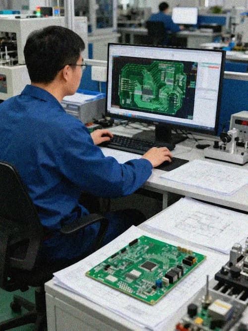
Edge AI boards are usually small, fast-moving, and constrained by industrial design. If a supplier only enters the process after Gerber release, its ability to reduce risk is limited. When procurement teams evaluate edge device PCB design services or AI embedded system PCB design partners, they should bring DFM review, stack-up recommendations, impedance simulation, thermal-path review, and pilot-run feedback into the same delivery flow. The earlier a supplier can identify conflicts among routing density, via size, material choice, and assembly tolerance, the lower the cost of the eventual design change.
Rigid-flex cracking in wearable or spatial computing products is a typical pilot-run problem. To save space, designers often place connectors, camera modules, and sensors in very compact regions, while the flex section must bend repeatedly during assembly. If bend radius, copper grain direction, coverlay openings, and stiffener placement are not reviewed during the PCB design stage, the prototype may power on successfully while reliability testing later shows resistance drift after several hundred bend cycles. Procurement teams that focus only on unit price can miss the schedule cost of rework, tool changes, and requalification.
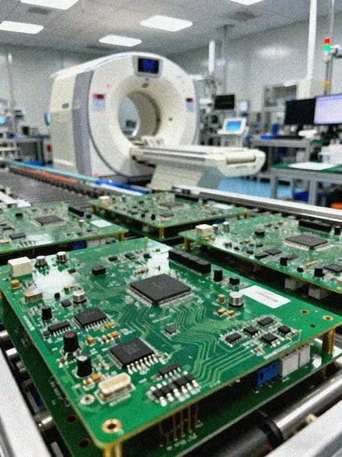
On-device AI also increases the value of quick-turn and small-batch capability. After WWDC26, developer teams and device brands are likely to validate new functions quickly, and hardware teams may need to iterate sensor boards, AI camera boards, or low-power edge computing nodes within weeks. Quick-Turn PCB Prototyping and Small Batch PCB Assembly can directly affect validation speed. The supplier needs fast prototyping capability, but it also needs the engineering discipline to convert prototype-stage issues such as impedance drift, BGA voiding, thermal hot spots, and EMI escapes into a stable manufacturing window.
On-device AI will not replace cloud compute, but it will redistribute PCB value
Apple’s official WWDC26 agenda puts AI, machine learning, and developer tools in a prominent position, while current media coverage is centered on Siri upgrades, AI developer platforms, and the wider rollout of Apple Intelligence. For the PCB industry, the value of this event is not in predicting the exact configuration of a future iPhone or Mac. The more useful signal is that on-device AI is pushing compute workloads into a wider range of terminal products. As local inference, real-time perception, and privacy-driven processing expand, board complexity in Edge AI Devices will continue to rise.
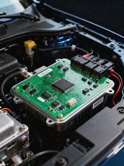
The supply-chain effect is practical rather than dramatic. AI server PCB demand remains concentrated in high-layer-count, high-speed, high-power boards. On-device AI creates a much more distributed set of compact projects: AI cameras, industrial edge gateways, medical monitoring devices, smart glasses, wearable sensors, and automotive cabin modules. The value of each individual board may be lower than that of an AI server main board, but the engineering difficulty can still be high because space, power, RF, thermal, and reliability constraints are compressed into a smaller product volume.
For suppliers with HDI, Rigid-Flex PCB, low-power edge computing board, and rapid NPI capabilities, WWDC26 offers a clear signal that competition in terminal AI features is moving back into hardware engineering detail. Over the next few months, procurement teams will likely ask more often about stack-up advice, impedance control, thermal simulation, pilot-run lead time, and batch consistency. PCB partners that can explain these issues during design and close the loop with data during pilot production will have a better chance of entering early supplier lists for on-device AI hardware programs.