Overview
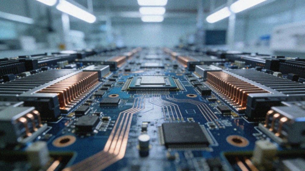
PCB prototyping is a critical pre-production link in electronic product R&D, designed to verify circuit design feasibility, identify signal integrity defects, thermal management loopholes, and manufacturing process incompatibility before mass production, effectively shortening product launch cycles and reducing overall R&D costs. With the continuous improvement of electronic product performance, modern prototyping services are no longer limited to simple single and double-sided board manufacturing, but need to adapt to the complex process requirements of high-speed transmission, high-density integration, and special material applications, covering everything from basic consumer electronic boards to high-precision IC substrates and high-speed optical communication boards, providing reliable verification carriers for R&D activities across all electronic industry segments.
Technical Capabilities
Our PCB prototyping services cover full-scene process requirements, with core capabilities including:
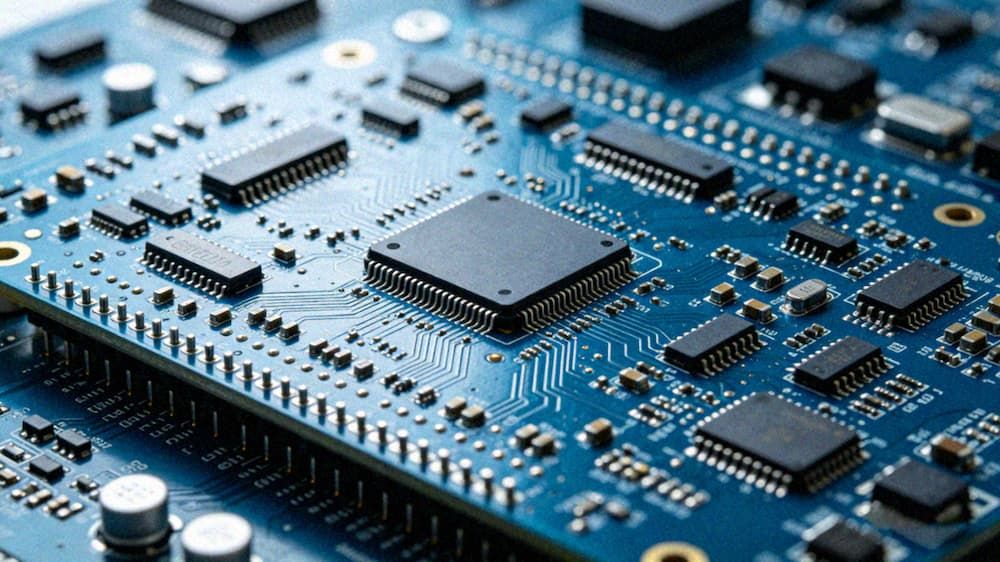
- Full Category Board Support: Support prototyping of all mainstream and special PCB types, including single-sided boards, double-sided boards, multilayer boards, HDI boards, rigid-flex boards, semi-flexible boards, high-frequency step boards, high-frequency hybrid boards, heavy copper boards, metal core/metal substrate boards, high-speed backboards, high-speed optical boards, ceramic boards, buried resistance/capacitance boards, buried copper block boards, buried ceramic boards, buried magnet boards, buried component boards, IC substrate boards, high-resistance carbon oil boards, and backlight mini-LED boards, adapting to diverse R&D needs across industries.
- Flexible Volume & Lead Time Configuration: Provide customizable prototyping volume options, from 1-piece small-batch functional verification to 500+ piece pre-production performance testing, with adjustable lead times based on board complexity, supporting 24-hour quick turn for simple double-sided and low-layer multilayer boards to meet urgent R&D schedule requirements.
- Design Value-Added Services: Provide full-chain design support including schematic review, stack-up planning, impedance matching, signal integrity simulation, and structural design optimization, covering ID design (appearance style, material, color matching, electromechanical coordination), structural design (material selection, process optimization, mold opening optimization, reinforcement, protective design), and interface adaptation (voice interfaces including I2C, TDM, PCM; power interfaces including DC, AC), helping customers optimize product performance, reduce manufacturing costs, and avoid subsequent design rework.
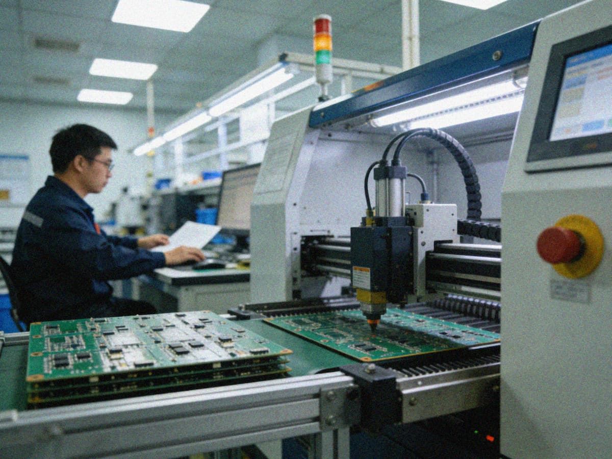
- High-Precision Process Control: Support mechanical blind and buried via, laser micro-via, and special lamination processes, with strict process control for line width/line spacing, hole position accuracy, and impedance tolerance, ensuring stable signal transmission for high-speed and high-frequency products, and 100% consistency between prototype performance and design specifications.
Quality Standards
All PCB prototyping services follow strict industry quality specifications, with core standards including:
- Material Compliance: All raw materials comply with RoHS, REACH, and other international environmental protection standards, with optional special materials such as high-frequency PTFE, high-thermal conductivity metal substrates, and high-temperature resistant ceramic substrates, adapting to harsh application scenarios such as high and low temperature, high humidity, and high corrosion.
- Full-Process Testing Verification: Each batch of prototypes undergoes multi-dimensional testing before delivery, including electrical continuity and insulation testing, impedance value verification, X-ray non-destructive testing for blind and buried via alignment, thermal cycle reliability testing, and appearance inspection according to IPC standards, ensuring zero functional defects of delivered products.
- Process Consistency Guarantee: All prototyping processes are consistent with subsequent mass production process specifications, strictly controlling parameters of lamination, drilling, plating, etching, and surface treatment processes, ensuring that prototype performance can be directly copied to mass production links, avoiding process adjustment risks during batch production transition.
Applications
PCB prototyping solutions are widely used in all electronic industry segments, including but not limited to:
- Consumer electronics: Smart wearable devices, mini-LED backlight displays, TWS audio equipment, and home intelligent terminals
- High-speed communication: 5G/6G base station communication boards, optical module boards, data center high-speed server backplanes, and network switch motherboards
- Industrial control: Industrial automation controllers, high-power power electronics, IoT sensing terminals, and new energy energy storage management boards
- Automotive electronics: ADAS perception system boards, smart cockpit core control units, and new energy vehicle BMS management boards
- High-end computing: AI edge computing equipment, IC package substrates, and high-performance computing server motherboards
- Medical electronics: Portable diagnostic equipment, medical monitoring terminals, and low-power implantable medical device circuit boards
- Aerospace: Satellite communication modules, avionics equipment, and industrial drone flight control system boards
Key Advantages
Compared with ordinary PCB manufacturing services, our prototyping solutions have the following core advantages:
- Cross-Industry Process Experience: Mature process accumulation for special board types such as high-frequency hybrid boards, buried component boards, and IC substrates, effectively solving common prototyping pain points including high-frequency signal attenuation, high-power board thermal management mismatch, and special material process incompatibility, with a 98% first-time prototyping success rate for complex special process boards.
- R&D Cost Optimization: Design-oriented service model provides process feasibility suggestions in the early design stage, helping customers avoid unnecessary high-cost process selection, and flexible volume configuration eliminates material waste caused by excessive minimum order quantity, reducing overall R&D investment by an average of 30%.
- Seamless Mass Production Docking: Prototyping processes are fully aligned with mass production lines, and we provide complete process parameter documents and mass production optimization suggestions after prototype verification is completed, supporting seamless transition from R&D verification to batch manufacturing, shortening the entire product launch cycle by more than 25%.
- Customized Demand Adaptation: Support customized requirements for special surface treatment, impedance tolerance, wide temperature resistance, and other special indicators, providing targeted solutions for niche and frontier R&D scenarios that cannot be met by standard prototyping services.
Contact Information
If you have customized PCB prototyping requirements for special materials, complex processes, or urgent lead times, you can contact our technical team at any time. We will provide you with free pre-prototyping technical evaluation, process feasibility analysis, and customized solution recommendations to support your efficient R&D activities.