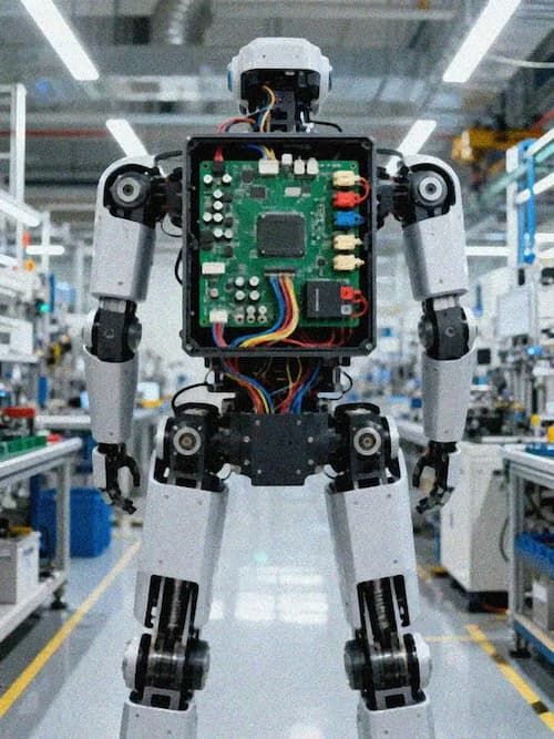
The Global Electronics Association report puts PCB factory AI in focus
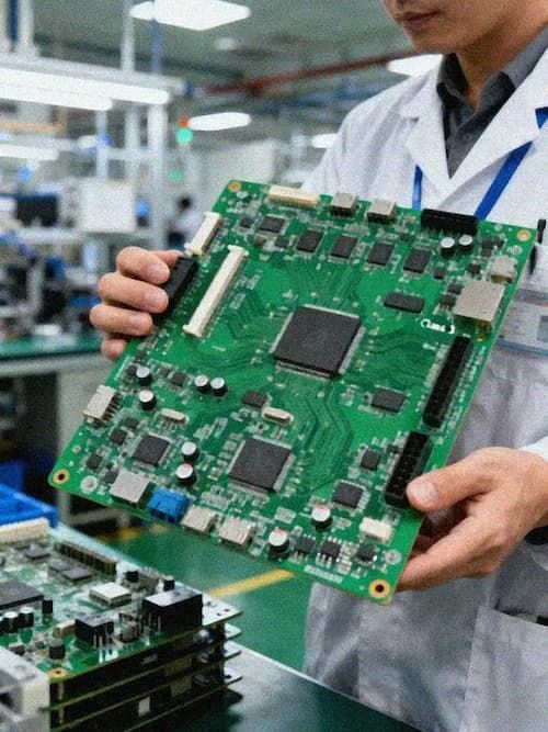
On June 8, the Global Electronics Association released its study, AI in PCB Manufacturing: From Pilots to Scale. The report covers major PCB manufacturing regions including mainland China, Taiwan, Southeast Asia, North America, and Europe, with a focus on where AI is already running, what business value it has produced, and what is required to move beyond isolated pilot projects. For the PCB industry, the useful part of this report is that it brings the discussion back to the factory floor: which processes are already producing measurable returns, and which problems remain tied to data, equipment, and organizational coordination.
Industry coverage on the same day, including reports from 21ic, EEWORLD, and CompoTech, centered on a practical distinction: AI adoption in PCB manufacturing is no longer unusual, while production-scale integration remains difficult. For suppliers, the discussion has moved beyond whether an AOI station can classify defects more quickly. The harder question is whether AI outputs can be connected to process records, equipment status, quality disposition, and engineering action in a way that improves the next production lot.
The manufacturing angle is broader than a single algorithm. Yield improvement, false-call reduction, root-cause analysis time, equipment stability, and data structure all matter because they affect how customers evaluate a PCB supplier during qualification and repeat orders. A factory can install AI inspection software and still struggle with inconsistent defect codes, incomplete equipment logs, or slow engineering feedback. In that situation, AI may improve one workstation while the wider quality system continues to depend on manual investigation.
AI AOI is moving first because the data loop is cleaner
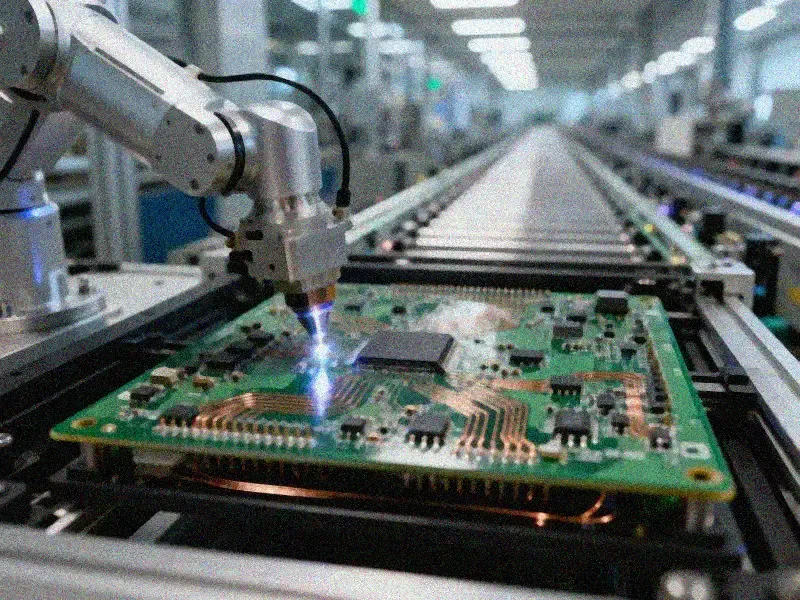
The report states that 68% of surveyed PCB companies have introduced AI into production operations, while adoption in China has reached 72%. Globally, only 8% of companies have achieved deep integration between AI and manufacturing systems. The most common application areas are process control, quality inspection and root-cause analysis, and product engineering. AI-enabled automated optical inspection (AOI) is one of the more mature entry points. According to the survey sample, AI AOI can improve yield by two to three percentage points, reduce reinspection rates by 30% to 40%, and shorten root-cause analysis time from six hours to two hours. These numbers matter for high-layer-count boards, HDI boards, and small-batch high-reliability programs.
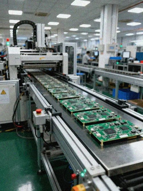
AOI has gained traction first because its data boundary is comparatively clear. Image data can be labeled, defect types can be linked to process steps, lots, and equipment status, and false calls or escapes can be fed back through reinspection results. Compared with cross-process issues in plating, lamination, and drilling, the AOI feedback loop is shorter. Engineers can determine more quickly whether the model is actually improving inspection efficiency, instead of simply adding another AI label to a production dashboard.
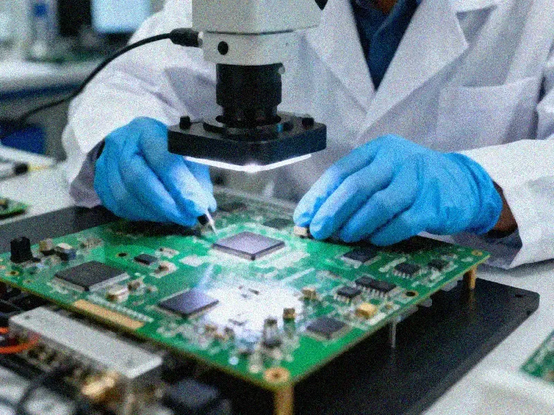
In real factories, AOI is not only about recognizing defects. On some high-density boards, post-etch inspection may show edge roughness, local trace narrowing, or copper residue. Traditional rule-based inspection often mixes acceptable process variation with actual defects, leaving reinspection teams to handle a large number of false calls. If an AI model lacks a stable sample library, it may drift when a new material, solder mask color, exposure tool, or surface finish is introduced. If reinspection results are not fed back quickly, the model can repeat the same classification mistake in the next lot. Procurement teams evaluating a supplier's AI AOI capability should look beyond whether the software module exists and ask whether defect classification, reinspection rules, engineering response, and lot traceability have formed a closed loop.
Scale-up depends on data consistency, equipment stability, and integration
The five scale-up challenges listed in the report sound familiar to anyone who has worked around a PCB shop floor: data quality and consistency, talent and capability gaps, unclear problem definition, system integration difficulty, and missing governance or ownership. These are manufacturing foundation issues, and algorithm tuning alone will not solve them. PCB production data comes from CAM, MES, AOI, flying probe test, electrical test, equipment sensors, warehouse systems, and quality platforms. If field names, timestamps, lot codes, and defect codes are inconsistent, an AI model cannot reliably trace a specific abnormality back to a specific process window.
Lamination and drilling provide a useful example. Many failures do not appear immediately at a single process step. Material expansion, lamination temperature profiles, inner-layer registration, drill offset, and hole-wall quality can interact, later showing up as opens, barrel cracking, CAF risk, or impedance deviation during electrical test, microsection analysis, or customer assembly. If data stays at the report level, engineers still have to investigate lot by lot based on experience. If equipment parameters, material batches, and inspection results are connected, AI has a better chance of narrowing the search area for the engineering team.
Equipment stability is another factor that is often underestimated. AOI systems, LDI tools, drilling machines, plating lines, and lamination presses all experience light-source degradation, mechanical offset, chemistry variation, and temperature fluctuation during long-term operation. These changes affect inspection images and process results. A model that performs well inside one stable window will not automatically adapt to every equipment condition. When maintenance records, calibration logs, and inspection results are disconnected, an AI system may classify equipment drift as product defects, or absorb real process abnormalities into normal variation.
Procurement should ask how AI enters the quality system
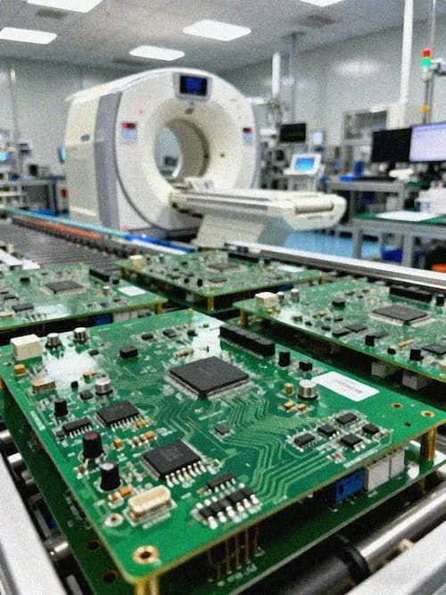
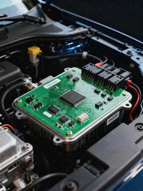
For procurement teams, AI in PCB manufacturing should become part of supplier audit logic, not a slide in a capability presentation. If a supplier claims to use AI AOI, buyers can ask for specific indicators: changes in reinspection rate, escape handling process, covered defect categories, model update frequency, manual review ratio, abnormal-lot traceability, and the boundary between AI judgment and final quality disposition. For automotive, medical, industrial, and energy customers, AI can support inspection and analysis, while final release still requires clear engineering sign-off and retained records.
During NPI, the value of AI tools is often in faster problem localization. A new HDI project moving from trial production into small-batch production may encounter microvia reliability variation, impedance deviation, BGA voiding, insufficient solder-mask bridge, or localized warpage. If a supplier can connect AOI defects, microsection results, electrical test failure points, process parameters, and DFM recommendations in one analysis chain, the customer's engineers can identify more quickly whether the issue comes from a narrow design window, an unsuitable material choice, or a factory parameter that needs adjustment. This kind of coordination has a direct schedule impact because one wrong root-cause call can lead to another trial build, fixture change, and requalification cycle.
Quality agreements also need to catch up. AI models are updated over time, and defect-disposition rules may change as the sample library grows. Customers therefore need clear requirements for change notification, data retention, abnormal-lot review, and traceability. For multinational customers, additional questions arise: whether production data can be shared across regions, whether the supplier can provide standardized reports, and whether different plants use consistent model logic and quality rules. Once AI enters the quality system, it affects customer audits, supplier grading, and long-term cooperation stability.
Smart manufacturing capability is becoming engineering infrastructure
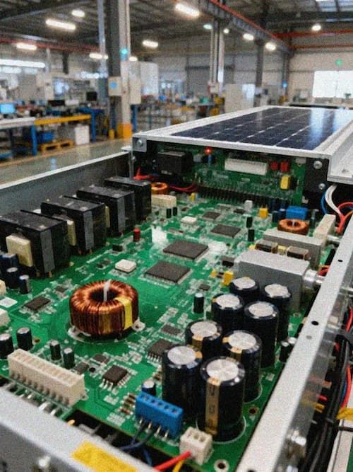
Another important signal from the Global Electronics Association report is that 81% of companies plan to increase AI investment over the next two to three years, with process optimization, production planning and operations, and quality inspection and analysis as priority areas. This direction overlaps with the increasing complexity of PCB products. AI servers, high-speed communications, on-device AI, industrial control, and medical electronics are all pushing layer count, line width and spacing, material combinations, and reliability requirements upward. A factory that still depends on scattered spreadsheets and individual experience will struggle to maintain stable delivery under a high-mix, low-volume, high-reliability order structure.
Smart manufacturing capability is becoming a form of engineering infrastructure. It includes data standards, equipment connectivity, defect libraries, process knowledge bases, quality traceability, cross-functional problem handling, and customer reporting. AI amplifies these foundations. If the underlying data is messy, the process window is unstable, or engineering experience cannot be captured, model deployment may create new communication costs rather than reducing them. For PCB suppliers, investment should focus on the full system from front-end engineering and manufacturing execution to quality review, with the algorithm platform as only one part of the architecture.
Over the next year, procurement audits of PCB factories are likely to become more specific. Traditional questions about capacity, certifications, equipment lists, and price will remain, but buyers may increasingly add AI AOI coverage, key-process data capture rate, abnormal-closure time, lot-to-lot consistency, and customer data interfaces. Suppliers that can turn AI applications into auditable, repeatable, continuously improving manufacturing capability will be better positioned in high-reliability PCB programs. Factories that keep AI at the demonstration level will find it difficult to offset real shop-floor variation with software claims alone.