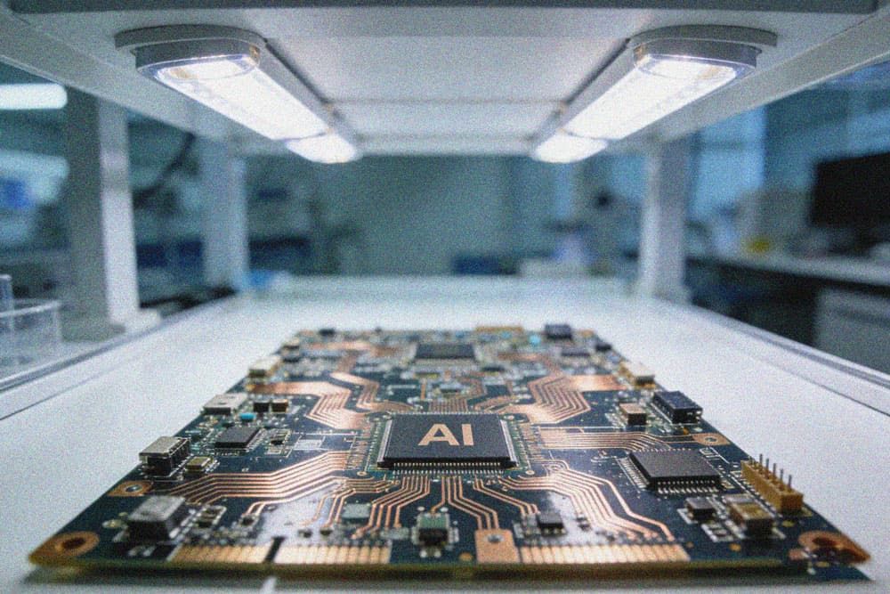
Overview
The rapid iteration of generative AI, industrial intelligence, and edge computing has put forward extremely strict requirements for the underlying hardware carrying AI computing loads. As the core carrier connecting computing chips, memory modules, high-speed interfaces, and power supply units, PCB design directly determines the stability of peak computing power, data transmission accuracy, and long-term service life of AI hardware. The dense deployment of 10-core+ CPUs, high-power GPUs/FPGAs, and high-bandwidth memory in AI computing systems often leads to common design challenges including high-speed signal attenuation, crosstalk between different signal layers, thermal accumulation under long-term full load, and voltage ripple of multi-voltage power distribution networks. Professional AI computing PCB design services cover the full process from schematic optimization, stack architecture planning, placement and routing adjustment, DFM (design for manufacturing) check, to performance testing and reliability verification, fully meeting the R&D and mass production needs of different types of AI computing hardware.
Technical Capabilities
- High-Layer High-Speed Signal Design Support: Supports 2 to 40+ layer PCB stack design, configurable with multiple independent power and ground planes to isolate signal interference between different layers. Achieves ±5% high-precision impedance control for 90Ω/100Ω differential signals, adapts to up to 750Gbps high-speed I/O transmission requirements, and supports common interface protocols including I2C, TDM, PCM, and high-speed optical interfaces, ensuring no distortion of high-volume data transmission between GPUs/FPGAs and high-bandwidth memory, and meeting the transmission needs of AI hardware with 16TOPS+ peak computing power.
- High-Density Routing and Special Process Compatibility: Supports micro-vias as small as 0.06mm and line width/space as low as 2.0/2.0mil, adapting to the high-density routing requirements of miniaturized AI computing modules. Compatible with a full range of special PCB processes, including buried resistance/buried capacitance boards, buried component boards, buried copper block boards, ceramic PCBs, high-frequency hybrid boards, mechanical blind and buried via boards, HDI boards, rigid-flex boards, and heavy copper boards, meeting the diversified design needs of different AI hardware scenarios.
- Targeted Thermal Management Optimization: For high-power AI computing hardware with thermal design power up to hundreds of watts, provides customized thermal design solutions, including embedded copper block heat dissipation structure, high thermal conductivity metal core board matching, and thermal pad placement optimization, reducing overall thermal resistance of the system by up to 30% compared with conventional designs, ensuring stable operation of computing chips under long-term full load.
- Power Integrity Optimization Design: Optimizes the power distribution network (PDN) for multi-voltage, high-current AI computing systems, reduces voltage drop and ripple noise, and supports DC/AC power supply design for multi-core computing units, ensuring stable power supply for high-power computing chips and peripheral components, and avoiding computing performance loss caused by unstable power supply.
- Full-Process Verification Support: Provides end-to-end verification services including signal integrity testing, power integrity testing, EMC testing, high and low temperature cycle testing, vibration and shock testing, fully verifying the reliability of design solutions before mass production, and reducing the risk of design rework.
Quality Standards
All AI computing PCB design processes strictly follow international industry standards including IPC-A-610 and IPC-6012, and selected materials comply with RoHS, REACH and other environmental regulations. For industrial-grade AI edge devices, designs support stable operation in the industrial-grade temperature range of -40℃ to +85℃, and meet the shock and vibration resistance requirements of outdoor and mobile deployment scenarios. All design outputs undergo three rounds of DFM checks to eliminate potential manufacturing defects in advance, improving the final mass production yield by more than 20% compared with unoptimized design solutions. For AI hardware with special safety requirements, designs can also meet corresponding industry compliance standards for industrial control, medical, and communication scenarios.
Applications
AI computing PCB design solutions can be widely adapted to various AI hardware scenarios, including but not limited to:
- **High-Performance AI Computing Modules: GPU/FPGA accelerator cards, edge AI core boards, 16TOPS+ high computing power visual processing boards, deep learning inference boards, and AI chip ATE test boards.
- **AI Infrastructure Hardware: High-speed backplanes for data center AI clusters, AI server motherboards, high-speed optical module PCBs for AI communication, and CLC interface boards for AI computing systems.
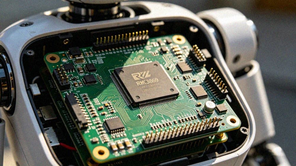
- **Industrial AI Edge Devices: Industrial robot main control boards, intelligent mechanical arm control boards, autonomous inspection robot core boards, power IoT AI monitoring units, and intelligent environmental monitoring terminal boards.
- **Smart AI Terminal Hardware: Intelligent home appliance main control boards, commercial intelligent interactive terminal PCBs, agricultural AI monitoring terminal boards, and 5G AI edge gateway boards.
Key Advantages
- **Full-Cycle Design Coverage: Covers the entire design chain from schematic optimization, stack planning, component placement, routing adjustment, DFM check, to prototype verification, reducing cross-stage communication costs, and shortening the hardware R&D cycle by 30% on average.
- **Manufacturing-Ready Design Matching: The design team masters the process parameters of all mainstream special PCB processes, eliminating the gap between design and manufacturing, ensuring that design solutions can be quickly converted into mass production without repeated adjustment, and reducing trial production costs.
- **Customized Scenario Adaptation: Provides targeted design optimization for different deployment scenarios, including industrial-grade wide temperature adaptation, dust and moisture protection design for outdoor edge devices, and low electromagnetic interference design for medical AI auxiliary equipment, meeting the diversified needs of different industries.
- **Cost-Optimized Design Support: Provides BOM optimization, component alternative recommendation, and process simplification suggestions during the design phase, reducing overall production cost by 15% to 25% without compromising product performance and reliability.
Contact Information
If you have AI computing PCB design requirements for high-performance computing cards, edge AI devices, or AI infrastructure equipment, you can reach out to our technical team to get free design feasibility evaluation, customized solution quotation, and professional technical consulting support. We will respond to your inquiry within 24 working hours, and provide targeted design solutions according to your specific performance, cost, and delivery requirements.