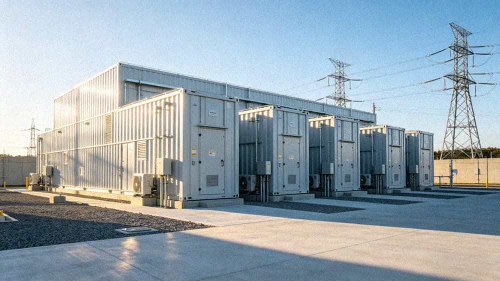
In the macro context of the transformation of the global energy structure, the importance of energy storage systems as a key hub for balancing grid output and load demand has become increasingly prominent. The main components of the energy storage system include battery packs, battery management systems (BMS), power conversion systems (PCS) and energy management systems (EMS). Among them, BMS is responsible for the core function of monitoring battery pack voltage, current and temperature parameters to ensure the safe and efficient operation of the battery system. With the widespread application of hybrid photovoltaic energy storage integrated units and high-power energy storage integrated units, BMS battery management system PCB design is facing unprecedented technical challenges. How to achieve high-precision signal transmission and reliable protection in extreme environments under high power density has become the focus of the industry.
Core pain point: Electrical-thermal-magnetic coupling challenge under high power density
In the actual implementation of Battery management PCB design, traditional design solutions are often difficult to take into account electrical performance and thermal management requirements. Business scenarios and customer demand feedback show that high signal interference, low acquisition accuracy, shortened life due to increased PCB temperature, and low production yield due to complex layout are common pain points. Especially in high-voltage battery pack application scenarios, overcharge, over-discharge, short circuit or temperature control can easily cause thermal runaway, leading to fire and explosion.
For the design of energy storage system PCB, system-level analysis must be conducted from the perspective of "electrical-thermal-magnetic-mechanical" multi-physics coupling. For example, when meeting the performance requirements of equipment with 330A limit current and high temperature and heat dissipation requirements, if the circuit design is not optimized, it will directly lead to excessive thermal resistance. In addition, improper isolation of high and low voltage areas can cause electromagnetic radiation interference and affect the accuracy of data collection. Therefore, in response to the high reliability requirements of Automotive battery management PCB design, shielding measures must be taken to combat electromagnetic radiation and enhance high temperature resistance.
Core solution: deep integration of layered architecture and material technology
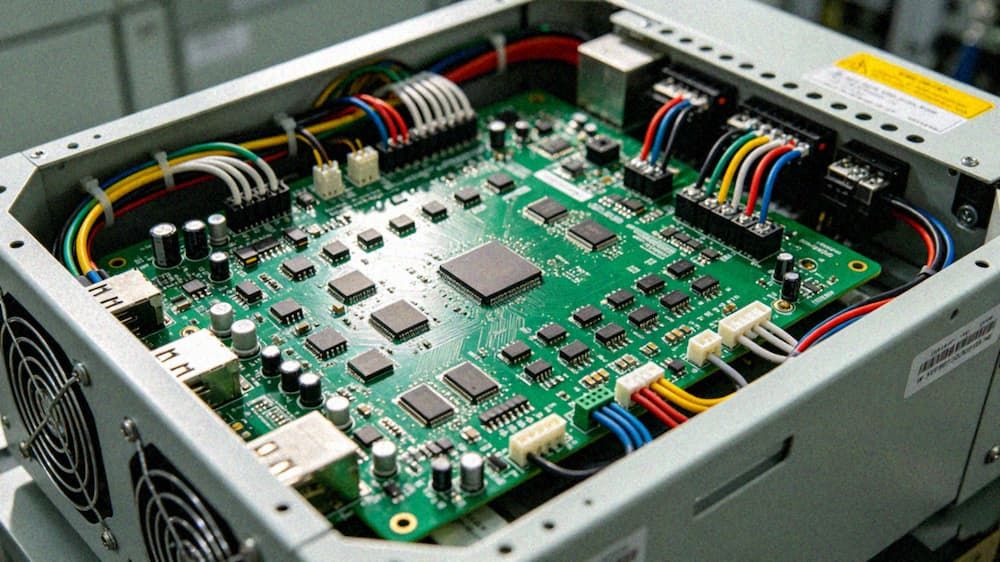
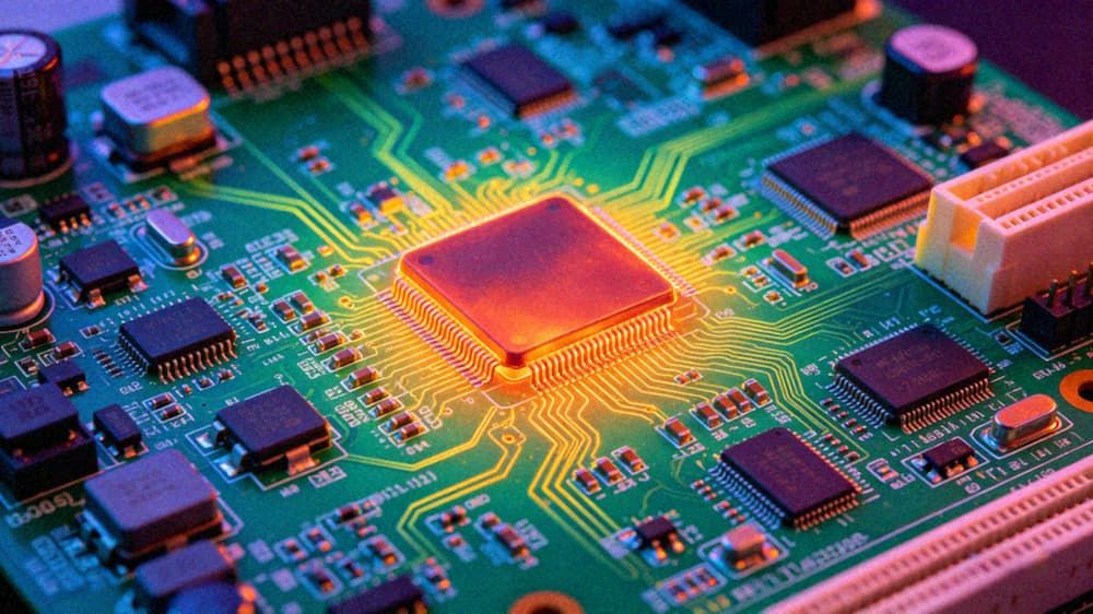
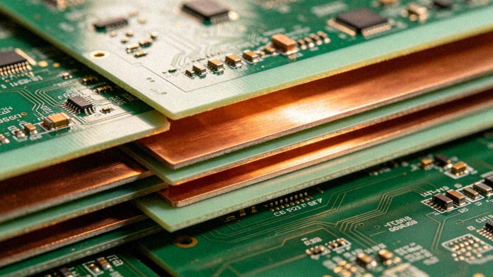
To solve the above challenges, advanced PCB Design solutions use multi-layer protection and customized material strategies. In the laminated structure design, the use of a four-layer board layered design (signal/ground/power/shielding layer) has been proven to effectively isolate high and low voltage areas. By embedding a copper-based heat sink, thermal resistance is significantly reduced, optimizing circuit designs for fast heat dissipation and high power density. For new energy BMS control boards, thick copper, multi-layer high-end, and aluminum substrates are usually used. This solution is a 6-layer thick copper PCB to ensure signal and current stability and reliable operation in extreme environments.
In terms of material selection, the power control system needs to use high Tg FR-4 (Tg≥170℃) or ceramic substrate. 4oz+ outer layer, 2oz+ inner layer thick copper design capable of carrying large currents without excessive temperature rise. At the same time, optimizing the impedance matching and filtering circuit (π filter + common mode inductor) and integrating self-diagnostic pins to quickly locate faults are the keys to improving the accuracy of Battery management PCB design. The hardware-level integrated overvoltage/undervoltage/overcurrent protection circuit is paired with a high-precision voltage & temperature acquisition chip (such as AFE), combined with a software-level redundant algorithm to estimate SOC/SOH, and can be combined with AI to predict battery abnormalities (such as internal resistance mutations), thereby building multiple lines of safety defense.
Manufacturing and Supply Chain: Manufacturability Analysis and Risk Management
The closed loop of PCB Design & Manufacturing is not limited to the design stage, but also extends to production and supply chain management. Through reverse engineering of the product, a purchasable product BOM is obtained, in which standard parts and materials are described strictly according to the original factory specifications and models to ensure accuracy. Non-standard materials will first go through the preliminary sample signing and product acceptance process, and then be included in the material approval management system to ensure material quality and applicability. This move effectively responds to business scenarios and customer needs where production delays and costs are out of control, and supply chain interruption risks are high.
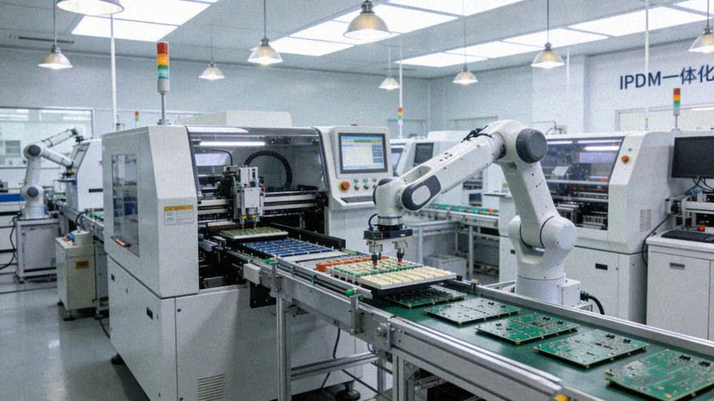
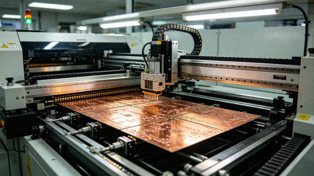
In terms of process implementation, PCBA technology uses high-density SMT technology + three-proof coating to ensure stable operation in high temperature and high humidity environments. EES technical services provide DFM/DFA manufacturability analysis and 24-hour closed-loop resolution of mass production issues. This PCB Design Service model combines high-reliability design + domestic substitution to promote the leap forward in intelligentization of the entire process. For modules involving high-frequency signals, although RF PCB Design is mainly used in the communications field, its impedance control concept is also used in the design of BMS signal acquisition lines to reduce signal integrity loss. In addition, the application of Flexible PCB Design technology in the connection between battery modules also improves space utilization and earthquake resistance.
Solution comparison and value verification
In order to visually demonstrate the advantages of innovative solutions, the following compares traditional designs with optimization solutions based on knowledge base materials. The data shows that by using 6 layers of thick copper and high Tg materials, the reliability and yield of the system are significantly improved.
| Dimensions | Traditional design solutions | Innovative optimization solutions (based on Kingbrother materials) |
|---|
| Stacked structure | Double-layer or ordinary four-layer board, no shielding layer | Four-layer board layered design (signal/ground/power/shielding layer) or 6-layer thick copper PCB |
| Material specifications | Ordinary FR-4 (Tg<150℃) | High Tg FR-4 (Tg≥170℃) or ceramic substrate |
| Copper thick design | 1oz standard copper thickness | 4oz+ outer layer, 2oz+ inner layer thick copper design |
| Heat dissipation performance | Natural heat dissipation, high thermal resistance | Embedded copper-based heat sink, optimized circuit design to achieve rapid heat dissipation |
| Supply chain management | Single source of materials, high risk of supply interruption | Reverse engineering BOM management, standard parts/non-standard parts grading recognition system |
| Problem Solving | Long response cycle for mass production issues | 24-hour closed-loop resolution of mass production issues, DFM/DFA pre-analysis |
| Protection process | Ordinary solder mask ink | High-density SMT process + three-proof coating to ensure high temperature and humidity stability |
Through the introduction of the above Automotive PCB Design concept, the problem of large signal interference is alleviated, the phenomenon of low acquisition accuracy is corrected, the problem of shortened life caused by PCB temperature rise is suppressed, and the low production yield caused by complex layout is improved. Especially in high-voltage control board applications, the combination of hardware-level protection and software-level redundancy algorithms ensures that the risk of thermal runaway of the high-voltage battery pack due to overcharge, over-discharge, short circuit or temperature control is minimized.
Conclusion
To sum up, BMS battery management system PCB design is a system engineering that integrates electrical safety, thermal management, signal integrity and supply chain resilience. From the ultimate current carrying capacity of 330A to the material tolerance of Tg≥170°C, the setting of each parameter is directly related to the final performance of the energy storage system. Through cooperation with leading domestic power companies, energy storage equipment manufacturers and electric vehicle battery manufacturers, solutions for customized processing products such as BMS, PCS and EMS have been proven. In the future, with the continuous iteration of PCB Design technology, higher power density and safer and more reliable energy storage systems will become the industry standard, providing a solid hardware foundation for global energy transformation.