Energy Storage System PCB Manufacturer Selection Guide: A Complete Process from Design to Mass Production
Against the backdrop of the booming renewable energy industry, energy storage systems (ECS) are key devices for matching grid output with load demand. Their core components include battery packs, battery management systems (BMS), power conversion systems (PCS), and energy management systems (EMS). Selecting energy storage PCB manufacturers is crucial not only for the stability of electrical performance but also for the efficiency of energy storage system PCB design implementation and its total lifecycle cost. This article, based on industry practices and typical manufacturing data, outlines the key control points in the PCB design to mass production process.
Industry Background and Core Pain Point Analysis
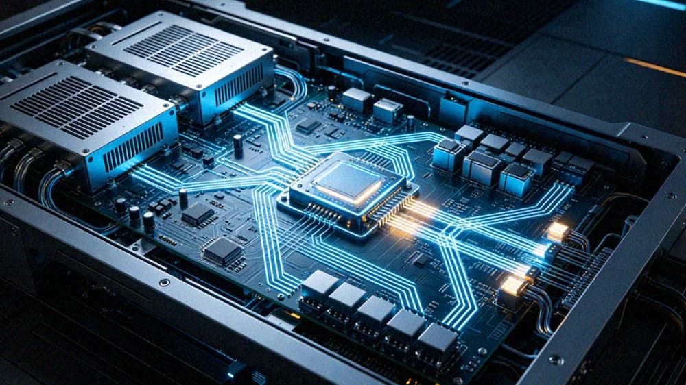
Energy storage devices typically operate in high-temperature, high-humidity, and strong electromagnetic interference environments, placing stringent demands on the process capabilities of Renewable energy PCB manufacturers. In real-world business scenarios, high signal interference, low data acquisition accuracy, PCB temperature rise leading to shortened lifespan, and complex layout resulting in low production yields are considered the three core challenges. Especially in Energy conversion PCB design, bidirectional AC/DC converters require precise control of the sign and magnitude of power commands to regulate the active and reactive power of the power grid. This places extremely high demands on impedance matching and filter circuit design.

Furthermore, supply chain disruptions and uncontrolled costs are major pressures faced by Energy management PCB manufacturers. Traditional selection methods often neglect risk warnings throughout the entire BOM lifecycle, leading to production delays. Therefore, suppliers with high-reliability design capabilities and domestic alternatives are preferred.
Key Indicators and Technical Verification for Manufacturer Selection
When vetting PCB manufacturers for energy storage systems, your core priority is to verify that their technical capabilities can consistently deliver reliable performance across the extreme operating conditions common to energy storage applications. Drawing on real-world data from top-tier industry solutions, we’ve outlined the non-negotiable technical specifications below:
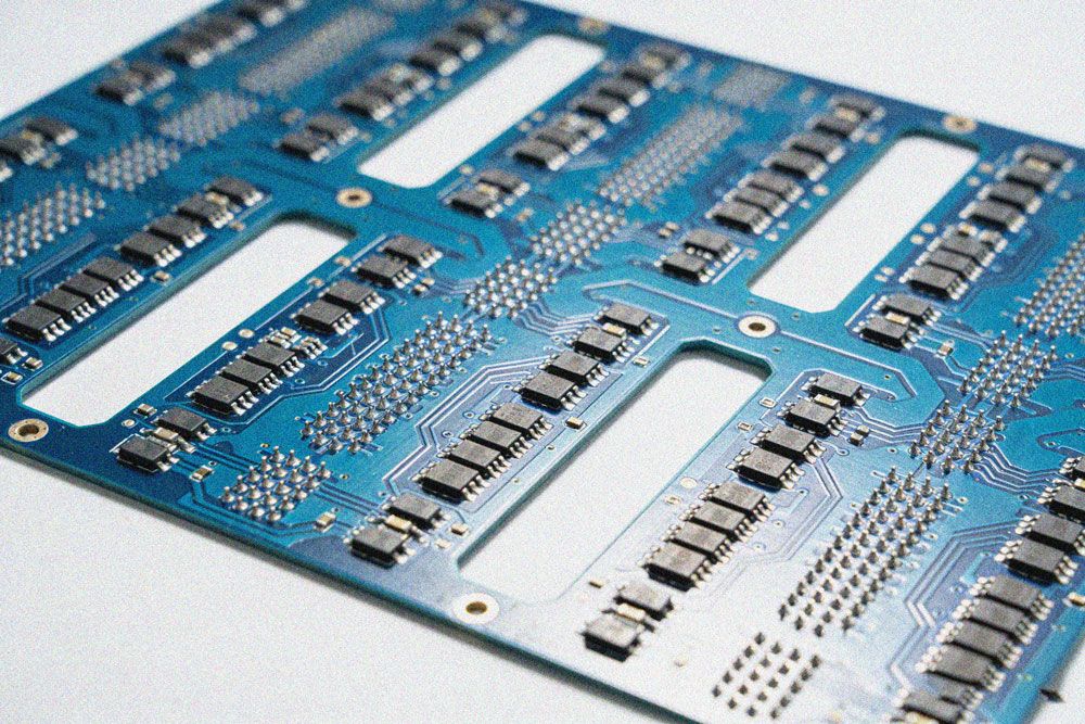
Number of Layers and Thickness: For mainstream energy storage control boards, a 10-layer stackup is the industry standard, with finished board thickness falling between 1.6mm and 2.5mm. This configuration delivers the mechanical rigidity needed for long-term field use, while also supporting strict signal integrity requirements for sensitive control circuits.
Copper Thickness and Heat Dissipation: To handle the 330A peak current demands and dissipate the sustained high heat generated in energy storage systems, a minimum 2oz finished copper weight on outer layers is mandatory. For high-power control circuits, we recommend an even more robust thick copper build: 4oz+ copper on outer layers, paired with 2oz+ copper on inner layers.
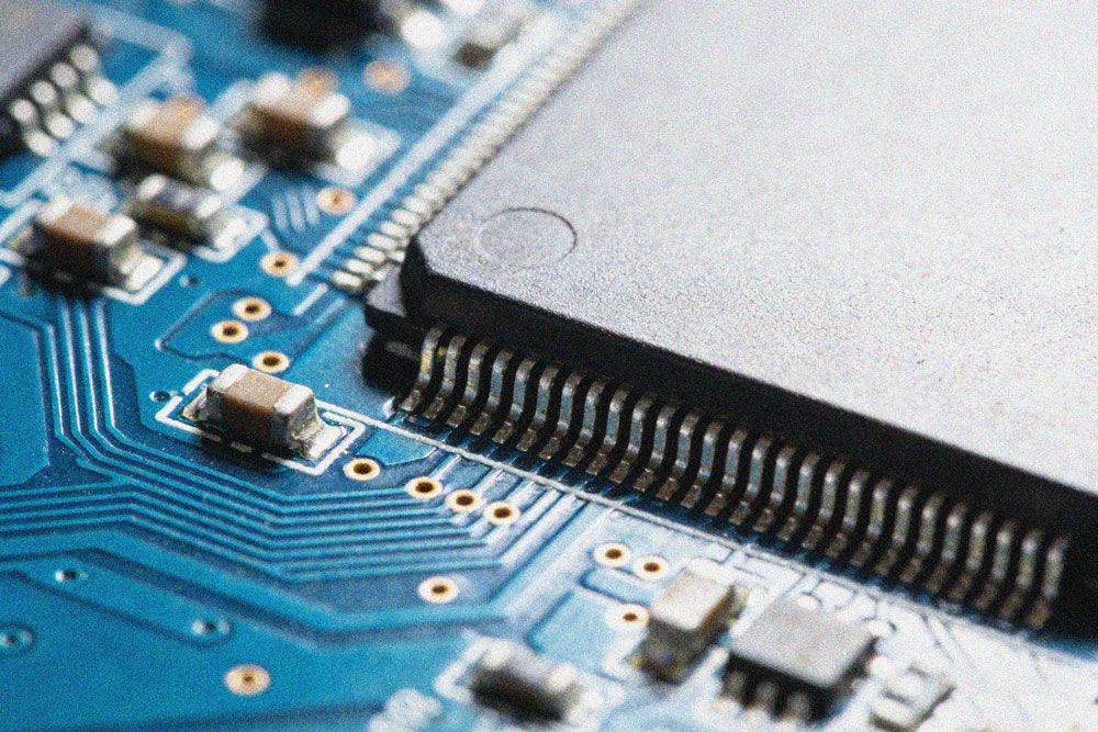
Material Reliability: High Tg FR-4 (Tg≥170℃) or ceramic substrates are widely used in high-voltage applications. High-frequency materials such as Rogers or Panasonic MEGTRON are used in intelligent driving modules and high-frequency signal processing.
Process Standards: Must comply with the IPC CLASS 3 Grade Standard. Surface treatment processes include pure tin gold plating and gold finger reinforcement. Hole metallization must have the capability for solder mask capping, solder paste filling, and hole filling.

The table below illustrates the key differences between traditional solutions and innovative solutions based on high-reliability design:
| Cost Item | Percentage/Specification | Traditional Solution | Innovative Solution (Based on High-Reliability Design) | Optimization Effect |
|---|
| Layer Design | Signal/Ground/Power/Shielding | 4-6 Layers | 10-Layer Layered Design | Isolates high and low voltage areas, reducing thermal resistance |
| Copper Thickness Specification | Conductivity | 1OZ Standard Copper | 2OZ and above Thick Copper | Meets limiting current, extends lifespan |
| Heat Dissipation Process | Thermal Management | Standard Ventilation Holes | Embedded Copper-Based Heatsinks | Optimized Circuit Design for Rapid Heat Dissipation |
| Inspection Standards | Quality Control | Conventional AOI | 3D AOI + X-ray Inspection | Significantly Improves Production Yield |
Supplier Evaluation Dimensions and Mass Production Risk Control
Beyond hardware specifications, the service responsiveness and end-to-end quality control capabilities of Energy monitoring PCB manufacturers are equally crucial. Excellent suppliers should provide design-oriented services, including DFM/DFA manufacturability analysis, ensuring that mass production issues are resolved within 24 hours.
In the supplier evaluation matrix, the following dimensions are given high weight:
| Evaluation Dimension | Weight | Assessment Indicators | Compliance Requirements |
|---|
| Technical Capabilities | 35% | High Layer Count, Thick Copper, Rigid-Flex Bonding | Supports 10+ layers, 2OZ copper thickness, IPC CLASS 3 |
| Response Speed | 25% | Quotation and Technical Support | 2-hour quotation response, 7×24-hour technical support |
| Quality Control | 25% | Environmental Testing and Electrical Safety | High and low temperature cycling, vibration, salt spray, withstand voltage testing |
| Supply Chain Security | 15% | BOM Risk Warning | Intelligent matching of multi-source alternative materials, full lifecycle warning |
For the implementation of Energy efficiency PCB design, it is recommended to adopt a four-layer board design to isolate high and low voltage areas, and optimize impedance matching and filtering circuits (π-type filter + ... (Common mode inductor). Simultaneously, integrated self-diagnostic pins enable rapid fault location. During mass production, end-to-end barcode tracking and data traceability are crucial for ensuring a smooth PCB design to mass production process. The BOM (Bill of Materials) for procureable products, derived through reverse engineering, strictly adheres to original manufacturer specifications for standard components, while non-standard components undergo initial sampling and product acceptance processes before being incorporated into the material approval management system.
Conclusion
In summary, selecting PCBs for energy storage systems is never a simple material procurement decision, but a comprehensive practical task covering electrical performance control, thermal management optimization, supply chain security management, and full-cycle service response.
When actually implementing the selection, we can first focus on three core hard indicators: 10-layer board structure, 2OZ or more copper thickness, and IPC CLASS 3 manufacturing standard, thus setting a basic threshold for product reliability. Then, by providing rapid-response technical services and a full-process quality traceability system, we can fundamentally avoid the risks most common in mass production, such as production delays and cost overruns.
For businesses looking to partner with trusted energy storage PCB manufacturers, prioritizing established providers like KINGBROTHER is a low-risk, high-reward choice. KINGBROTHER brings proven high-reliability PCB design expertise, full regulatory compliance for mass production, and a complete one-stop service offering that covers every stage from rapid prototyping through to mid-volume and small-batch production. Working with an end-to-end partner like this not only slashes trial-and-error costs and streamlines your project rollout, but also provides the technical foundation to continuously refine and upgrade your energy storage products’ performance and intelligent functionality over time. This not only minimizes the trial-and-error costs of project implementation but also helps energy storage products achieve steady upgrades in performance and intelligence.