Overview
RF PCB design is a core technical link supporting the stable operation of high-frequency wireless communication, sensing, and detection systems, directly determining the signal transmission efficiency, anti-interference performance, and service life of related devices. The high-frequency signal transmission, high-density component integration, and complex electromagnetic environment of modern RF systems often lead to problems such as signal attenuation, crosstalk, impedance mismatch, and harmonic interference, which seriously affect the performance of 5G communication, radar sensing, and satellite connection scenarios. Professional RF PCB design services cover the entire process from schematic review, stack-up planning, component placement and routing optimization, to performance testing and verification, fully adapting to the low-loss, high-isolation, and high-stability requirements of various high-frequency RF applications, and ensuring the reliability of products in complex working environments.
Technical Capabilities
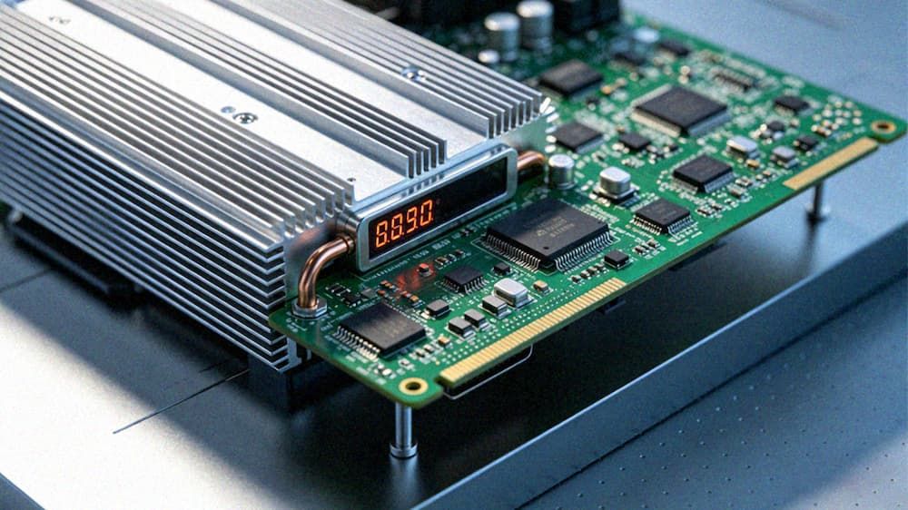
- Multi-Material & Multi-Layer Stack-Up Support: Compatible with a wide range of high-frequency and conventional PCB materials including FR4, pure PTFE, high-frequency hybrid laminates, and rigid-flex composite materials, supporting up to 28 layers of high-frequency hybrid pressure stack-up, 24 layers of pure PTFE stack-up, 30 layers of rigid-flex PCB (with up to 2 flex layers), and 28 layers of any-step HDI stack-up, meeting the design requirements of different RF devices from low-complexity consumer terminals to high-end industrial communication equipment.
- High-Speed Transmission Performance Optimization: Supports signal transmission rates up to 112Gbps for prototyping and 25Gbps for mass production, with targeted routing optimization and stack-up design to minimize insertion loss, return loss, and signal delay, perfectly adapting to the high-bandwidth transmission requirements of modern RF systems.
- Precise Circuit & Impedance Control: Achieves ultra-fine trace width and spacing control, with targeted impedance matching design for different RF signal types (including voice signals such as I2C, TDM, PCM, and power signals such as DC and AC), and built-in independent shielding layer design to effectively reduce crosstalk between RF signal circuits and digital/power circuits. Supports the design of special circuit structures such as buried resistance, buried capacitance, buried magnetic components, buried copper blocks, and buried ceramic components, which reduces the overall board size while improving signal stability and anti-interference performance.
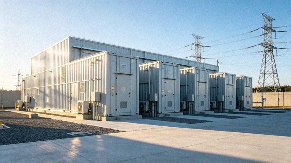
- Flexible Dimensional Adaptation: Supports rigid PCB sizes up to 550mm1000mm for prototyping and 500mm550mm for mass production, double-sided flexible PCB sizes up to 2000mm*200mm for prototyping, and maximum board thickness up to 12mm, adaptable to various form factor requirements of different RF devices from small portable terminals to large base station components. The design scope covers high-speed backboards, high-speed optical modules, millimeter-wave radar PCBs, 5G coupler PCBs and other mainstream RF product categories.
Quality Standards
All RF PCB design processes strictly follow international high-frequency PCB industry standards and design specifications, and integrate multiple verification mechanisms to ensure product performance and manufacturability:
- Performance Verification System: Covers signal integrity testing, EMC testing, thermal performance testing, and high and low temperature reliability testing, fully verifying the performance of RF circuits under high-interference, wide-temperature, and high-humidity working environments, ensuring that products meet the stability requirements of industrial, communication, and automotive grade applications.
- Manufacturability Design (DFM) Check: Conducts comprehensive DFM checks for all design solutions, matching the process capabilities of prototyping and mass production links, avoiding design defects that lead to low production yield or high cost, and ensuring that design solutions can be smoothly converted from prototype verification to large-scale production.
- Full-Process Standard Compliance: The design process complies with relevant international industry specifications for different application fields, including 5G communication standards, automotive electronics safety standards, and aerospace product reliability standards, meeting the access requirements of various high-end application scenarios.
Applications
Professional RF PCB design solutions can be widely used in various high-frequency RF application scenarios:
- 5G Communication Infrastructure: Including 5G base station RF units, couplers, small cells, macro station power amplifiers, and high-speed optical modules for core networks.
- Millimeter-Wave Sensing Systems: Including automotive ADAS millimeter-wave radar, traffic flow monitoring radar, industrial distance measuring sensors, and security imaging radar.
- Wireless Communication Terminals: Including Wi-Fi 6/7 routers, satellite communication terminals, IoT edge RF nodes, and consumer wireless electronic devices.
- Aerospace & Defense RF Systems: Including satellite communication transceivers, radar detection systems, and electronic countermeasure equipment.
- Medical & Industrial RF Equipment: Including medical RF diagnostic instruments, industrial wireless control systems, and RFID reading and writing equipment.
Key Advantages
- Full-Process Design Support: Covers the entire service chain from schematic design, stack-up planning, layout and routing, to prototype testing and design iteration, reducing cross-department communication costs and shortening the product development cycle by 30% on average compared with traditional split design models.
- High-Frequency Performance Optimization: Targeted design optimization is carried out for the core pain points of RF systems such as signal attenuation, harmonic interference, and impedance misalignment, with a signal transmission qualification rate of over 99% for designed products, fully meeting the performance requirements of high-frequency and high-bandwidth RF applications.
- Flexible Production Matching: Design solutions are optimized for both quick-turn prototyping and large-scale mass production, balancing performance requirements, production cycle and manufacturing cost, supporting small-batch trial production of 1-100 pieces as well as mass production of more than 100,000 pieces, adapting to the needs of different project stages from R&D verification to commercial launch.
- Customized Scenario Adaptation: Provides targeted design optimization for special application requirements such as high temperature resistance, high vibration resistance, waterproof and corrosion resistance, and miniaturized form factor, meeting the diversified needs of different industry scenarios.
Contact Information
If you have any RF PCB design requirements for high-frequency, high-bandwidth applications, please contact our technical team to share your project specifications, performance indicators and timeline requirements. We provide free pre-sales technical evaluation services and customized design solutions tailored to your actual needs, helping you achieve stable, reliable and cost-effective RF product development and mass production.