Overview
Flexible PCB design is a core link in the development of modern miniaturized, lightweight, and high-performance electronic products, directly determining the electrical performance, structural adaptability, and long-term reliability of flexible circuit boards. Unlike rigid PCBs, flex PCBs require balancing dynamic bending resistance, electrical signal stability, and manufacturability, with common design challenges including signal attenuation during repeated bending, impedance mismatch for high-speed transmission, copper layer fatigue failure, and interlayer compatibility for rigid-flex hybrid structures. Our flexible PCB design services cover the full end-to-end process from schematic review, stack-up architecture planning, component placement optimization, routing adjustment, design for manufacturing (DFM) checks, to pre-production reliability simulation, supporting all standard and custom flex PCB configurations to meet the needs of diverse industry use cases from prototype development to large-scale mass production.
Technical Capabilities
We offer comprehensive flexible PCB design technical support covering all mainstream configuration types and performance requirements:
- Wide Configuration Support: Covers single-sided flex, double-sided flex, 2-12 layer multi-layer flex, rigid-flex, semi-flex, high-frequency hybrid flex, and HDI flex designs, adapting to different structural and electrical requirements of electronic products.
- Precise Impedance and Signal Integrity Optimization: Supports impedance control accuracy of ±5% for 50Ω, 90Ω, 100Ω specifications, with dedicated signal integrity simulation to minimize crosstalk, attenuation, and reflection for high-speed transmission up to 112Gbps PAM4, meeting the demands of high-bandwidth data transmission.
- Bending Fatigue Optimization: Provides targeted material selection, routing path design, and copper thickness adjustment solutions, supporting dynamic bending cycles up to 10,000 times and static bending radius as small as 3x the board thickness, avoiding circuit breakage or performance degradation during long-term use.
- High-Density Design Compatibility: Supports line width/line spacing as small as 2.0/2.0mil, micro-via diameter down to 0.06mm, and blind/buried via configurations, adapting to the miniaturization needs of compact electronic devices with limited internal space.
- Comprehensive DFM and Verification Support: Includes pre-production design for manufacturing, design for assembly (DFA), and design for testing (DFT) checks, plus reliability simulation for temperature shock, vibration, and humidity resistance, reducing prototype iteration cycles by up to 30% and lowering mass production defect rates.
- Special Material Adaptation: Supports design for special flexible substrates including high-frequency PTFE flex materials, high-temperature resistant modified polyimide, and biocompatible medical flex materials, meeting the needs of niche high-end application scenarios.
Quality Standards
All flexible PCB design processes follow universal industry standards to ensure design compatibility and product reliability:
- General Design Specification Compliance: Aligns with IPC-2223 flexible PCB design standards, IPC-4204 flexible material performance standards, and IPC-A-600 acceptability standards for printed boards, ensuring design consistency across different manufacturing facilities.
- Industry-Specific Standard Alignment: Adapts to sector-specific requirements including IATF 16949 for automotive electronics, ISO 13485 for medical devices, and AS9100 for aerospace applications, meeting the strict compliance requirements of regulated industries.
- Manufacturing Process Compatibility: Design parameters are fully compatible with mainstream flexible PCB manufacturing processes including laser drilling, LDI direct imaging, cover film lamination, and ENIG/OSP surface treatment, avoiding design-induced manufacturing failures.
- Reliability Testing Alignment: Design specifications are validated against standard reliability testing requirements, including thermal cycling (-40℃ to +125℃), 1000+ hour humidity resistance testing, and EMC compliance testing, ensuring end products meet required performance thresholds.
Applications
Flexible PCB design solutions cater to a wide range of high-end electronic application scenarios, including but not limited to:
- Consumer Electronics: Foldable smartphones, wearable devices (smart watches, fitness trackers), TWS earphones, laptop hinge components, and camera module connectors
- Automotive Electronics: ADAS sensor connectors, smart cockpit display flexible connections, battery management system (BMS) components, and autonomous driving domain controller internal interconnections
- Medical Devices: Portable diagnostic equipment, implantable medical sensors, surgical robot components, and wearable health monitoring devices
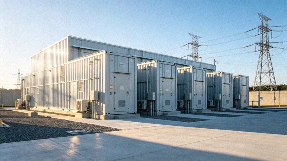
- Industrial and Aerospace: Industrial control sensor wiring, drone internal interconnections, satellite communication module components, and portable military electronic equipment
- High-Speed Communication: 5G base station RF components, high-speed data cable connectors, and optical module internal flexible interconnections
- Lighting and Display: Mini LED backlight flexible boards, flexible OLED display driver boards, and smart lighting module interconnections
Key Advantages
Our flexible PCB design services offer distinct value for product development teams:
- End-to-End Design Support: Covers the full product lifecycle from initial schematic review, prototype design optimization, small-batch trial production adjustment, to mass production design standardization, reducing cross-stage communication costs and iteration time.
- Performance and Cost Balance: Optimizes material selection, stack-up structure, and routing design based on actual application scenarios, avoiding over-design while ensuring required electrical performance and reliability, reducing overall product development and manufacturing costs by 15-25% on average.
- Customized Scenario Adaptation: Provides targeted design solutions for specific usage scenarios, such as high-temperature resistance for industrial applications, biocompatibility for medical devices, and anti-vibration performance for aerospace use cases, meeting diverse industry-specific requirements.
- Fast Iteration Capability: Standardized design processes and pre-built material and component libraries enable fast prototype design delivery within 3-5 working days for urgent projects, supporting rapid product launch for customers.
Contact Information
If you have flexible PCB design requirements for prototype development, small-batch trial production, or mass manufacturing, please reach out to our technical team. We will provide you with customized design solutions, free DFM evaluation, and professional technical consulting services tailored to your specific project needs.