Overview
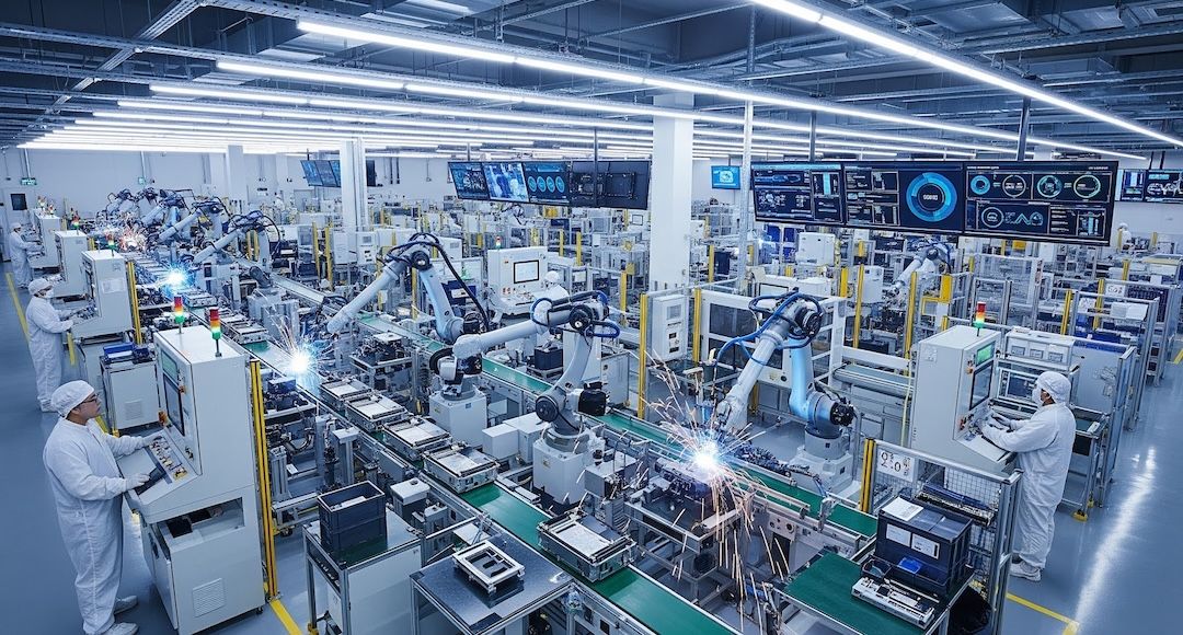
PCB fabrication is the foundational process for all electronic hardware, directly impacting the performance, reliability, and lifespan of end products across every industry. As electronic designs grow more complex, with demands for higher density, faster signal transmission, better thermal management, and adaptability to harsh operating environments, fabrication processes must evolve to support advanced design specifications without compromising yield or cost efficiency. Our full-spectrum PCB fabrication capabilities cover the entire production lifecycle from rapid prototyping and small-batch validation to high-volume mass production, supporting both standard and custom specialty board requirements to address the most demanding electronic design challenges.
Technical Capabilities
Our fabrication processes are optimized to support a wide range of board types, advanced processing techniques, and tight tolerance specifications to align with diverse project needs.
Supported Board Types
We fabricate all standard and specialty PCB categories, including:
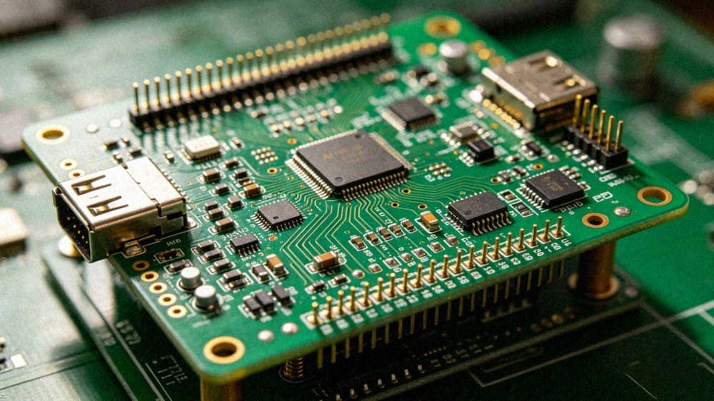
- Standard rigid boards: Single-sided, double-sided, and multilayer boards up to 40 layers, suitable for most general electronic applications
- High-density interconnect (HDI) boards: Supporting micro-via and stacked via designs for high-density consumer electronics and computing hardware
- Flex and rigid-flex boards: Including semi-flexible boards, ideal for wearables, aerospace, and compact electronic devices with form factor constraints
- High-performance boards: High-frequency boards, high-frequency hybrid boards, high-speed backplanes, and high-speed optical boards optimized for 5G/6G telecom, high-speed networking, and AI computing systems
- Specialty functional boards: Heavy copper boards for high-power applications, metal core/metal substrate boards for enhanced thermal management, ceramic boards, buried copper block boards, buried ceramic PCBs, high-resistance carbon oil boards, backlight mini-LED boards, substrate boards, and IC substrate boards for semiconductor packaging applications
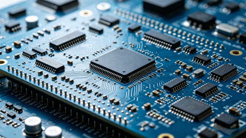
Advanced Process Capabilities
We support a full suite of cutting-edge fabrication processes to accommodate complex design requirements:
- Blind and buried vias, stack vias, via-in-pad, and epoxy fill for high-density routing
- Back drilling, depth control drilling, countersink, and step slot processing for high-speed signaling and mechanical fit requirements
- Embedded copper and embedded component integration for improved thermal performance and reduced board footprint
- High-frequency hybrid material integration for cross-function performance optimization
- Long and short gold connector plating, half-hole processing, laser cutting, and carbon ink application for specialized functional requirements
- Mixed surface finish options to align with application-specific reliability and assembly needs
Manufacturing Tolerance Specifications
Our production lines are calibrated to deliver consistent high precision, with the following core specifications:
- Minimum pitch accuracy of 0.5mm, supporting minimum component packages as small as 01005 (0.3mm * 0.2mm) for ultra-compact designs
- Standard board thickness support from 0.5mm to 3mm, with custom support for thicknesses outside this range for specialized applications
- Maximum board dimensions up to 600mm (length) * 450mm (width), with support for unconventional size specifications within semi-automatic production capacity
- Double-sided assembly support for component heights up to 25mm, accommodating large SMD components up to 200mm * 125mm
Quality Standards
All fabrication processes adhere to strict international industry quality standards, including IPC-A-600 acceptability criteria for printed boards and IPC-6012 performance specifications for rigid PCBs. Every production batch undergoes multi-stage quality validation, including raw material inspection, in-process dimensional accuracy testing, impedance control verification, thermal cycling testing, humidity resistance testing, and electrical continuity testing to ensure consistent performance across operating environments. For high-reliability applications, optional third-party validation services are available to meet industry-specific compliance requirements for automotive, medical, aerospace, and industrial end uses.
Applications
Our PCB fabrication capabilities are widely applied across a diverse range of industry use cases:
- Telecommunications: High-frequency and high-speed boards for 5G/6G base stations, routers, and signal transmission equipment
- Automotive electronics: Heavy copper, rigid-flex, and high-temperature resistant boards for autonomous driving domain controllers, smart cockpit systems, and power management units
- Consumer electronics: HDI, mini-LED backlight, and semi-flex boards for smartphones, wearable devices, home entertainment systems, and display panels
- Industrial control: Metal core and heavy copper boards for industrial automation equipment, power converters, and high-temperature operating environments
- Medical devices: Biocompatible, high-reliability boards for diagnostic equipment, patient monitoring systems, and implantable device components
- Aerospace and defense: High-vibration resistant, wide-temperature range boards for avionics systems, satellite components, and defense communication equipment
- Semiconductor and computing: IC substrates and high-speed backplanes for AI servers, edge computing nodes, and semiconductor testing equipment
Key Advantages
Choosing our PCB fabrication services delivers multiple core benefits for your hardware development projects:
- Full spectrum board support: Covers all standard and specialty board types in a single production partner, eliminating the complexity of managing multiple vendors for mixed design requirements
- High precision process control: Tight tolerance control for high-density and high-speed designs minimizes signal loss, impedance mismatch, and manufacturing defects, ensuring your design performs as intended
- Scalable production capacity: Seamlessly supports rapid prototyping runs of 5 units or less up to high-volume mass production of 100,000+ units, with consistent quality and yield across all batch sizes
- Design for manufacturability (DFM) support: Our engineering team provides free DFM reviews prior to production to identify and resolve potential manufacturing issues early, reducing iteration costs and shortening project timelines
- Custom process adaptation: Supports non-standard size, thickness, and process requirements for specialized applications, with flexible production workflows to accommodate custom design requests
Contact Information
If you have custom PCB fabrication requirements for your electronic hardware project, reach out to our technical support team for a free feasibility assessment and customized quote. Our engineering experts will work with you to optimize your design for manufacturability, align production specifications with your performance and cost targets, and deliver high-quality PCB solutions that meet your project timeline and reliability requirements.