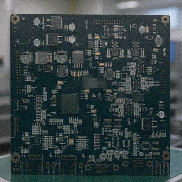
Overview
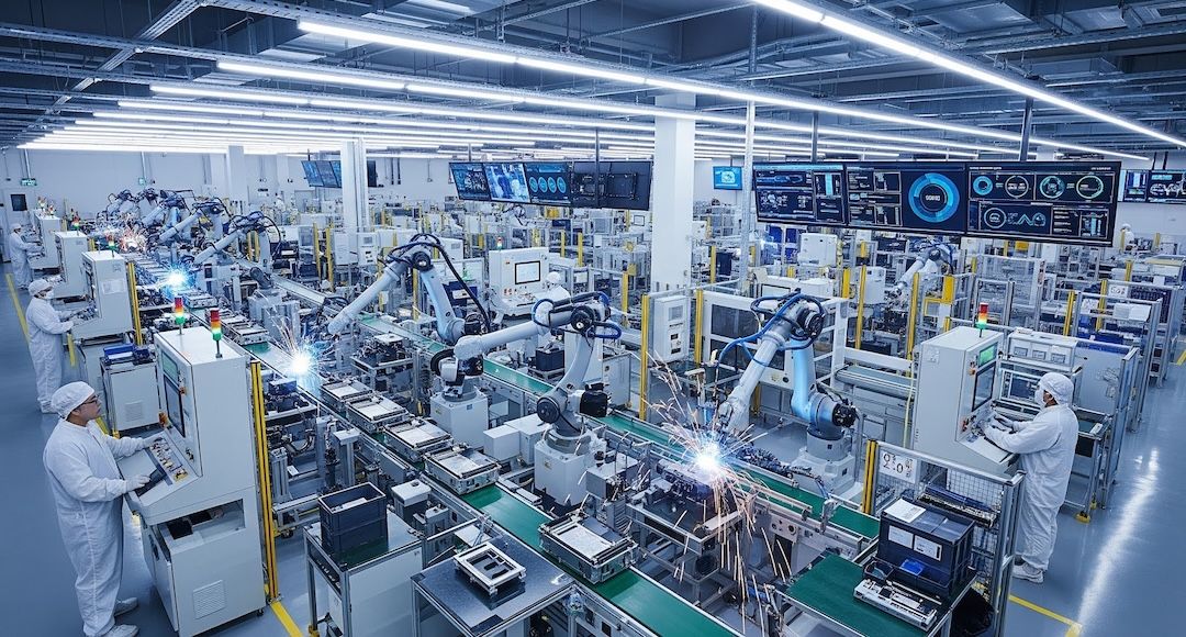
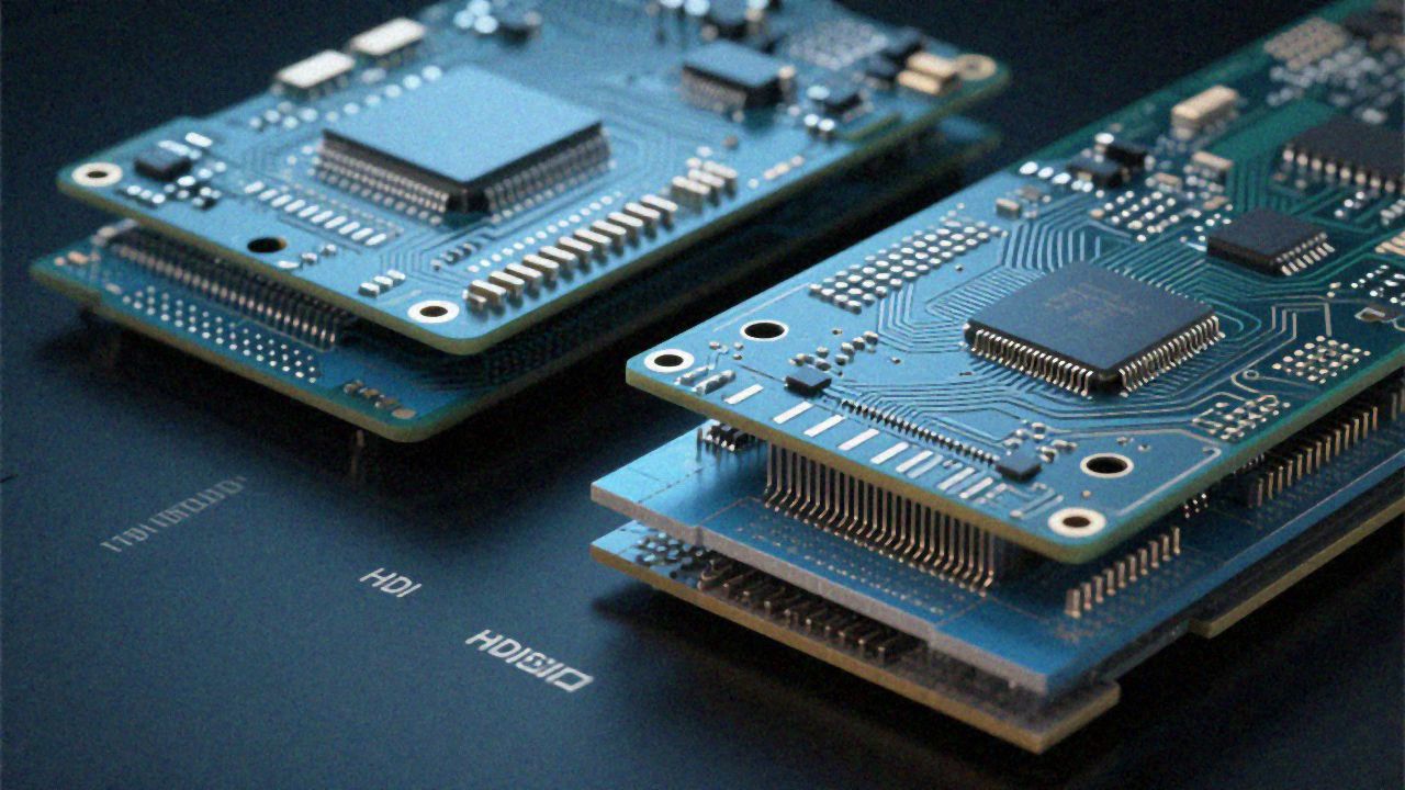
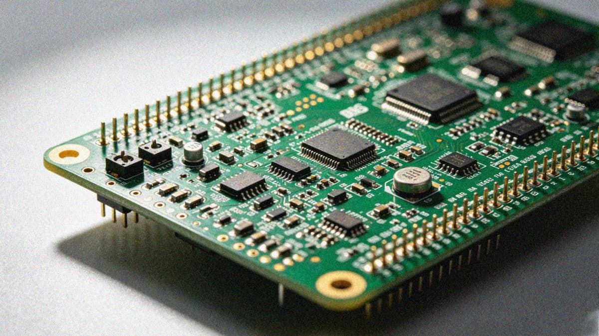
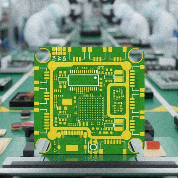
High-Density Interconnect (HDI) PCB is a core printed circuit board solution designed to meet the miniaturization and high-performance demands of modern electronic products. As electronic devices continue to shrink in form factor while integrating more functional components and supporting higher data transmission rates, traditional multi-layer PCBs can no longer meet the requirements of high routing density, low signal loss, and stable performance. HDI PCBs use micro-via, blind/buried via, and stacked via technologies to achieve higher component placement density, shorter signal transmission paths, and better signal integrity, addressing core industry pain points such as limited routing space, high signal attenuation, and poor thermal dissipation in compact device designs. These boards are widely recognized as the preferred solution for high-end electronic products across multiple regulated and high-growth sectors.
Technical Capabilities
HDI PCB manufacturing capabilities cover a wide range of technical configurations to adapt to diverse project requirements:
- Layer and Interconnection Support: Offers HDI PCB configurations up to 28 layers with any-layer (any step) interconnection, plus 1 to 4 step stacked via options for 20-layer HDI designs, accommodating complex routing requirements for high-density surface mount component placement.
- Specialized HDI Variant Coverage: Supports multiple customized HDI types including thick copper HDI, high-frequency HDI, MINI LED backlight HDI, and blind/buried via mechanical HDI, adapting to specific performance demands such as high current load, high-frequency signal transmission, and dense LED array integration.
- High-Speed Transmission Adaptation: Supports data transmission rates up to 112Gbps, with precise impedance control accuracy within industry-leading tolerance ranges, effectively minimizing signal reflection, crosstalk, and attenuation to meet the requirements of high-bandwidth low-latency data transmission scenarios.
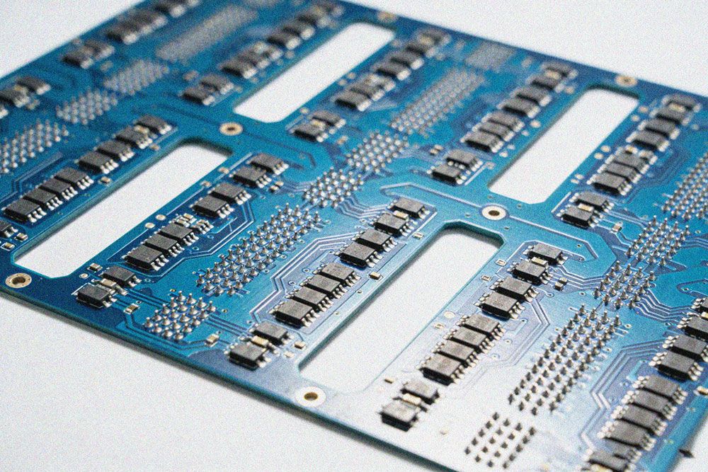
- Ultra-Precision Manufacturing Tolerances: Enables production of fine trace width/spacing as low as 2.0/2.0mil, with micro-via diameters down to 0.06mm, ensuring high routing density and signal stability for ultra-miniaturized device designs.
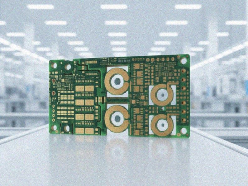
- Wide Material Compatibility: Works with a broad range of substrate materials including standard FR4, high-frequency mixed pressure substrates, pure PTFE, and ceramic-filled composites, optimizing for thermal conductivity, dielectric constant consistency, and mechanical stability for different use cases.
- Customized Parameter Adjustment: Supports customized configurations for copper thickness (up to 10OZ for thick copper HDI), board thickness (up to 12mm), and board size (up to 550mm*1000mm for rigid HDI) to match unique product form factor and performance requirements.
Quality Standards
All HDI PCB products adhere to strict industry quality control frameworks to ensure long-term stable performance in demanding operating environments:
- Incoming Material Validation: All substrates, copper foils, dielectric materials, and plating chemicals undergo pre-production testing for thermal resistance, dielectric constant consistency, peel strength, and mechanical toughness to eliminate performance deviations caused by material defects.
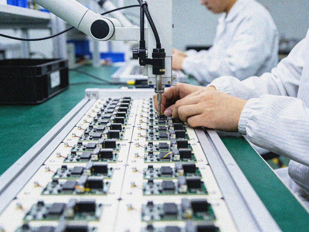
- In-Process Full Inspection: Implements 100% inspection at key manufacturing stages including laser drilling, lamination, etching, and plating, with X-ray non-destructive testing to verify via alignment, interconnection integrity, and lamination bonding quality.
- Finished Product Performance Testing: All finished HDI boards undergo a full suite of reliability tests including signal integrity testing, thermal cycling testing (-40℃ to +85℃), impedance verification, insulation resistance testing, and solderability testing, ensuring compliance with international IPC PCB performance standards.
- Regulatory Compliance Alignment: Production processes align with ISO9001, IATF16949, ISO13485 and other industry-specific quality system requirements, making products suitable for regulated sectors such as automotive, medical, and aerospace with strict access thresholds.
Applications
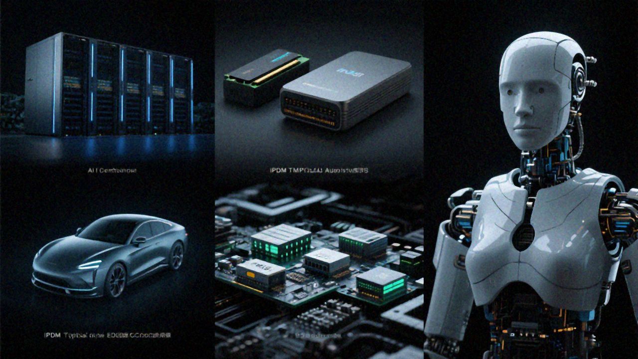
HDI PCB solutions are widely deployed across multiple high-growth electronics sectors, including:
- Communication Equipment: 5G couplers, 25G/100G/400G optical modules, millimeter-wave radar boards, base station core control units, and high-speed backplanes, supporting high-bandwidth, low-latency data transmission for 5G and next-generation communication networks.
- Medical Electronics: Gene sequencing equipment, superconducting magnetic resonance imaging (MRI) systems, HRV monitoring devices, and portable diagnostic tools, requiring high reliability, biocompatibility compliance, and stable performance in medical-grade operating environments.
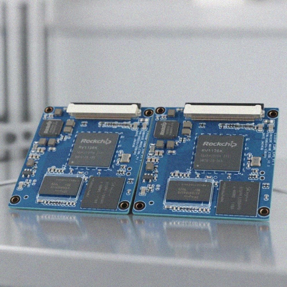
- Consumer Electronics: Mini LED backlight displays, wearable smart devices, high-end smartphones, tablet computers, and AR/VR devices, supporting compact design, high component density, and low power consumption requirements.
- Automotive Electronics: Autonomous driving domain controllers, smart cockpit core units, in-vehicle sensor systems, and vehicle-to-everything (V2X) communication modules, adapting to wide temperature ranges, high vibration, and high electromagnetic interference operating conditions.
- Industrial Electronics: Industrial edge computing nodes, high-speed industrial control motherboards, intelligent inspection equipment, and industrial IoT terminals, ensuring long-term stable operation in harsh industrial environments with high dust, humidity, and temperature fluctuation.
Key Advantages
Choosing professional HDI PCB solutions delivers multiple core benefits for product development and mass production:
- High Design Flexibility: Supports fully customized configurations for layer count, via structure, material selection, copper thickness, and surface treatment, adapting to unique performance and form factor requirements of different projects, from small-batch prototypes to large-scale mass production.
- Reliable Performance Guarantee: Optimized stack design and precision manufacturing processes ensure consistent signal integrity, thermal dissipation efficiency, and mechanical stability, reducing product failure rates over the entire service lifecycle by more than 30% compared to traditional multi-layer PCBs.
- Cost Optimization: Mature manufacturing processes and high production yield enable cost-effective solutions for both prototype small-batch production and large-scale mass production requirements, balancing performance and cost to help clients improve product market competitiveness.
- Full Cycle Technical Support: Covers the entire product lifecycle from design for manufacturing (DFM) consultation, prototyping, performance testing, to mass production, reducing product iteration time and cross-stage communication costs for clients, shortening time-to-market by 20% on average.
Contact Information
If you have HDI PCB design or manufacturing requirements for your project, please reach out to our technical support team. We offer free DFM evaluation, customized solution drafting, and professional technical consulting services to help you meet your product performance, budget, and timeline goals. Our team will respond to your inquiry within 24 working hours.