Overview
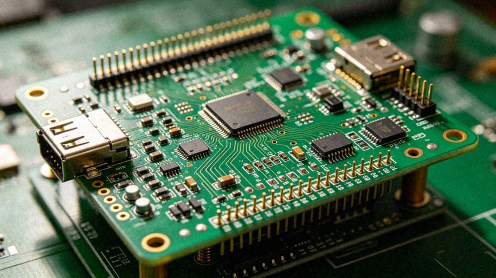
AI sensor hardware serves as the core data input terminal for AI systems, responsible for collecting, preprocessing, and transmitting real-time data from vision, LiDAR, temperature, motion, and other sensing modules. Unlike conventional consumer electronics PCBs, AI sensor PCBs face unique technical challenges: high-density layout of computing chips and sensing components can easily cause signal crosstalk, high-load operation of AI edge computing chips leads to concentrated heat generation, and low-latency data transmission requirements put forward strict standards for impedance control and signal integrity. Specialized AI sensor PCB manufacturers deliver end-to-end design and production solutions tailored to these pain points, supporting the full lifecycle of AI sensor hardware from R&D prototyping to large-scale mass production, with flexible order policies to adapt to projects of different scales.
Technical Capabilities
AI sensor PCB production covers a comprehensive set of technical processes to meet diverse performance and form factor demands across application scenarios:
- Full Board Type Support: Covers single/double-sided boards, 2-40+ layer multilayer boards, HDI boards, rigid-flex boards, heavy copper boards, high-frequency hybrid boards, metal core/substrate boards, high-speed backboards, buried ceramic PCBs, embedded component (capacitor, resistor, active component) boards, and semi-flexible boards, adapting to the miniaturization, high-heat, and high-frequency demands of different AI sensor products.
- High-Speed Signal Design & Manufacturing: Supports high-speed I/O transmission up to 750Gbps, with configurable stack-up designs featuring up to 4 independent ground planes to shield cross-layer signal interference, achieving 90Ω/100Ω impedance control accuracy within ±5% tolerance, meeting low-latency, low-loss transmission requirements for AI sensor raw data and computing output signals.
- High Thermal Stability Design: Supports heavy copper (up to 20oz copper thickness) and metal core/ceramic substrate board production, with optimized thermal routing and copper pouring designs to dissipate heat generated by high-power AI computing chips and sensing modules, ensuring stable operation under continuous high-load conditions.
- Embedded Component Integration Capability: Supports embedded capacitor, resistor, and active component embedding processes, reducing board footprint by up to 35% compared to conventional surface mount designs, adapting to the miniaturization demand of portable and edge AI sensor terminals.
- Flexible Production Scale Support: Covers fast prototyping, small-batch trial production, and large-scale mass production, with no minimum order quantity requirements, supporting R&D verification, pilot run, and full commercialization stages of AI sensor hardware projects without additional cost burden for small-scale test orders.
Quality Standards
All AI sensor PCB production processes follow international industry standards, with full-process quality control covering incoming material inspection, manufacturing process monitoring, and post-production performance testing:
- Cross-Industry Compliance Alignment: Production processes align with ISO 9001 quality management, IATF 16949 automotive quality, ISO 13485 medical quality, and RoHS environmental protection standards, adapting to compliance requirements for AI sensor products applied in industrial, automotive, medical, and consumer scenarios.
- Full-Item Testing Verification: Perform a full set of reliability tests including signal integrity testing, thermal cycling testing (-40℃ to +85℃), EMC testing, vibration and shock testing, X-Ray non-destructive testing, and impedance testing, ensuring 100% of delivered products meet pre-defined design specifications.
- Full Traceability Process Control: Implement end-to-end traceability for all production processes, with real-time monitoring of key parameters such as line width/spacing (minimum 2.0/2.0mil supported), micro-via diameter (minimum 0.06mm supported), and plating thickness, ensuring batch consistency of mass-produced products and reducing post-sales failure risks.
Applications
AI sensor PCB solutions are applicable to a wide range of AI-driven sensing and computing hardware scenarios, including but not limited to:
- Industrial AI Sensing Systems: Industrial robot master control boards, mechanical arm sensing control boards, ATE equipment test boards, intelligent environment monitoring sensors, power transmission and control boards, and thyristor control units
- Edge AI Terminal Devices: Intelligent home appliance master control boards, IoT handheld devices, intelligent security dynamic identification sensor boards, intelligent audio control boards, and smart retail terminal sensing modules
- Autonomous System Sensors: Autonomous service robot master control boards, intelligent agricultural mowing robot sensing boards, logistics autonomous transport vehicle LiDAR control boards, and commercial vehicle autonomous driving perception system boards
- High-Performance AI Computing Hardware: GPU/FPGA solution boards, high-performance computing cards, optical module boards, 5G antenna boards, and high-layer high-speed backplanes for AI server systems
Key Advantages
Partnering with professional AI sensor PCB manufacturers brings core value to AI hardware R&D and production projects:
- Full-Chain Service Coverage: Provides end-to-end services covering schematic design optimization, stack planning, BOM optimization, component procurement and management, PCB manufacturing, PCBA assembly, and performance testing, eliminating cross-vendor communication costs and reducing project R&D cycles by up to 30%.
- AI Scenario Customization Support: Offers targeted design optimizations for specific AI sensor application scenarios, including high dust and moisture resistance designs for industrial outdoor environments, wide temperature adaptability designs for automotive and outdoor IoT scenarios, and miniaturization designs for consumer edge terminals.
- High Yield Guarantee: Equipped with advanced production equipment including laser drilling machines, LDI laser direct imaging systems, and automatic optical inspection equipment, achieving a production yield of over 98% for complex high-density AI sensor PCBs, reducing manufacturing costs for mass production projects.
- Full Lifecycle Technical Support: Assigns a dedicated technical team to support every project from demand evaluation to after-sales service, providing real-time technical consultation and problem solving for design, manufacturing, and testing stages, helping teams resolve technical bottlenecks quickly.
Contact Information
If you have custom AI sensor PCB manufacturing needs, including fast prototyping, small-batch trial production, or large-scale mass production, please reach out to our technical team. We will provide you with a free technical evaluation, targeted solution design, and transparent quotation services to support the smooth launch of your AI sensor hardware projects.