Overview
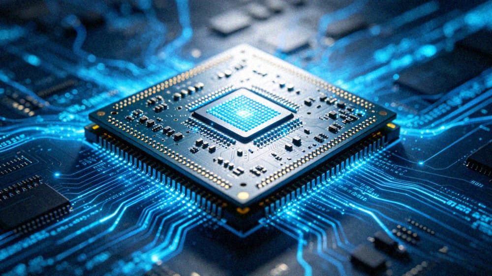
Medical AI PCB design is a core technical link supporting the stable and reliable operation of AI-powered medical devices, which face far stricter performance and safety requirements than consumer or industrial electronic products. The deployment of high-computing chips such as GPUs, FPGAs, and dedicated AI SoCs for medical image analysis, real-time physiological signal processing, and surgical robot control brings multiple design challenges, including high heat generation, high-speed signal attenuation, crosstalk, and impedance misalignment, which may directly affect diagnostic accuracy, surgical safety, and patient monitoring data reliability. Professional medical AI PCB design covers the full process from schematic design, stack-up planning, placement and routing optimization, to performance verification, addressing core pain points of medical AI hardware R&D, and ensuring products meet clinical use and regulatory compliance requirements.
Technical Capabilities
- High-speed high-density design support: Supports design of up to 40-layer high-speed backplanes, HDI boards, and high-layer count boards for high-computing medical AI hardware, compatible with 16TOPS+ AI chip deployment, and supports up to 750Gbps high-speed I/O transmission to meet low-latency processing demands of high-resolution medical image analysis and real-time diagnostic algorithms. It also supports micro-vias as small as 0.06mm and line width/space down to 2.0/2.0mil, enabling high-density component placement to reduce the overall size of portable and wearable medical AI devices.
- Optimized heat dissipation design: Supports design of heavy copper boards, buried copper block boards, buried ceramic boards, and metal core substrate boards, which effectively reduce thermal resistance by more than 30% compared with standard PCB designs, avoiding performance throttling or device failure caused by overheating of high-power computing chips under long-term continuous operation in clinical scenarios. It can be customized for natural convection, forced air cooling, or liquid cooling matching schemes according to product usage scenarios.
- Rigid-flex and special structure adaptation: Supports design of rigid-flex boards, semi-flexible boards, buried component boards, and buried resistance/capacitance boards, adapting to the structural requirements of wearable AI monitors, minimally invasive surgical robot control boards, and other form-factor constrained devices. It also supports design of rigid-flex boards with gold finger reinforcement for high-plug-cycle medical test equipment interface boards, improving service life of frequently plugged interfaces.
- High-precision signal integrity control: Achieves ±5% high-precision impedance control for 90Ω and 100Ω differential signals, and supports stack-up design with up to 4 independent ground planes to shield signal crosstalk, suppress electromagnetic interference, and ensure zero-error transmission of high-resolution medical image data and patient physiological signal data, avoiding diagnostic misjudgment caused by signal distortion.
- Full-process design verification: Provides end-to-end verification services covering signal integrity testing, EMC testing, thermal cycling testing, biocompatibility material testing, and high/low temperature reliability testing, validating design performance across the full range of clinical operating environments from 0℃ to 60℃, meeting 24/7 long-term operation requirements for in-hospital medical AI equipment.
Quality Standards
- All design processes comply with IPC-A-610 medical-grade electronic assembly standards and IEC 60601 international medical device safety regulations, ensuring basic safety and effectiveness of medical AI device circuit systems.
- Design processes strictly follow medical device EMC requirements, with electromagnetic radiation levels controlled below the specified threshold to avoid interference with other in-hospital medical equipment such as MRI, ECG monitors, and life support systems.
- Material selection follows biocompatibility requirements for devices in direct or indirect contact with patients, meeting ISO 10993 material testing standards for wearable, implantable, and surgical medical AI devices, avoiding adverse reactions between the circuit board and human tissue.
- All design outputs include complete traceability documentation, supporting medical device full lifecycle traceability requirements for clinical audit and post-market surveillance, meeting the regulatory filing requirements of medical device products in major global markets.
Applications
Medical AI PCB design solutions can be widely applied to various AI-powered medical device scenarios, including:
- AI-assisted diagnostic imaging equipment: Core boards for CT, MRI, X-ray, and ultrasound AI analysis systems, supporting high-speed transmission of high-resolution image data and low-latency AI algorithm inference for real-time lesion identification and auxiliary diagnosis.
- Surgical robot control systems: Master console control boards, robotic arm end effector control boards, and image transmission boards for minimally invasive surgical robots, supporting high-precision signal transmission and low-latency feedback to ensure surgical operation accuracy.
- Wearable AI patient monitors: Dynamic ECG, blood glucose, and multi-parameter vital sign AI analysis monitors, with rigid-flex board design adapting to wearable form factors, low-power design supporting long-term continuous monitoring, and accurate collection and analysis of physiological signal data.
- Point-of-care testing (POCT) AI devices: AI analysis boards for rapid diagnostic test of infectious diseases, cardiac markers, and other test items, supporting fast data processing and result output, adapting to use requirements of primary care, emergency, and field medical scenarios.
- In-hospital AI monitoring systems: Intelligent ward patient monitoring central boards, AI fall detection terminal control boards, and medical image data transmission backplanes, supporting stable long-term operation and high-bandwidth data transmission for multi-device connection.
Key Advantages
- End-to-end one-stop design service: Covers the full chain from schematic design, stack-up planning, component placement and routing optimization, prototyping, to testing and verification, with support for BOM optimization and component selection guidance, reducing cross-stage communication costs, ensuring design manufacturability, and avoiding rework delays caused by design and manufacturing mismatches.
- Scenario-specific customized design: Provides targeted design solutions for different medical AI device scenarios, including low-power design for portable devices, high heat dissipation design for high-computing fixed equipment, and miniaturized design for implantable or wearable devices, fully meeting differentiated product R&D requirements.
- Mature high-computing chip adaptation experience: Extensive design experience adapting to mainstream high-computing chips for medical AI applications, including FPGA, GPU, and dedicated AI SoC chips, supporting matching of AI compiler tools and SDK kits to accelerate product R&D and validation cycles, shortening time to market by an average of 20%.
- Full-cycle production support: Supports small-batch prototype verification, medium-batch trial production, and large-scale mass production requirements, with consistent design performance across different production batches, ensuring stable product quality during production scaling.
Contact Information
If you have medical AI PCB design requirements for diagnostic, monitoring, surgical, or other medical AI hardware applications, you can reach out to the professional technical support team for customized design solutions, free technical evaluation, and professional consulting services tailored to your specific project needs.