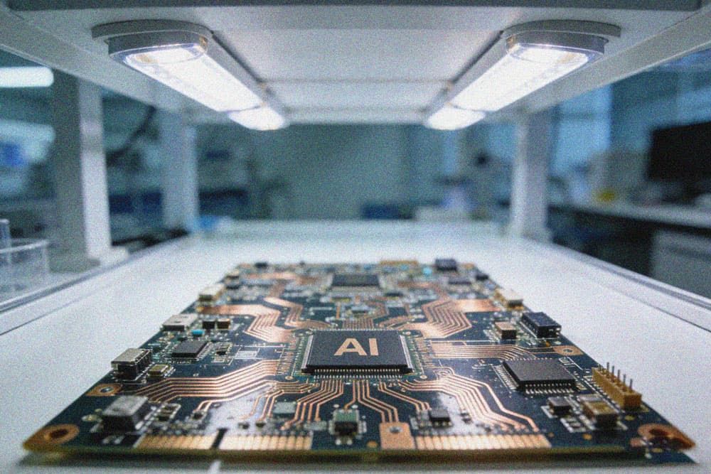
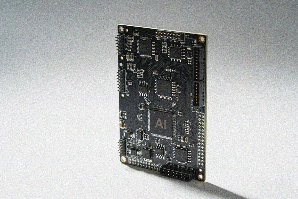
Overview
AI PCB advanced packaging is a core enabling technology for high-performance AI hardware, addressing the performance bottleneck between advanced AI chips and system-level boards caused by increasing computing power, I/O density, and bandwidth demands. As AI chips move towards 7nm and smaller process nodes, traditional packaging architectures can no longer meet the requirements of low signal transmission loss, high thermal dissipation efficiency, and high interconnection density. Advanced PCB packaging technologies integrate high-density interconnection structures, high-speed material matching, and precision process control, effectively shortening the signal transmission path between chips, reducing power consumption, and improving the overall performance and reliability of AI computing systems. It is widely used to support the packaging of high-power AI processors, GPU modules, and high-speed AI server components, providing a reliable hardware foundation for AI training clusters, edge computing devices, and intelligent application terminals.
Technical Capabilities
AI PCB advanced packaging solutions cover a full range of process capabilities to meet diverse AI hardware design requirements:
- Multi-layer Stacking Support: Supports 12 to 32 layer PCB designs for advanced packaging, compatible with high-TG FR4, TU933+ high-speed low-dielectric materials, and hybrid high-frequency material lamination. The stack design can be customized with independent ground planes and power planes to shield signal interference, adapt to different signal transmission rates and thermal performance requirements, and meet the impedance control needs of high-speed differential signals and high-bandwidth memory interfaces.
- High-Density Interconnection Process: Supports 0.2mm minimum through-hole, 0.06/0.075mm (2.5/4.5mil) line width/line spacing, second-order stacked via + mechanical blind hole structures, BGA laser fill holes and resin via-in-pad processing. These processes enable higher I/O density in a smaller board area, matching the dense pin layout of advanced 7nm and 5nm AI chips, reducing the overall packaging size while improving interconnection reliability.
- Special Process Control: Equipped with metalized slot and press-fit hole precision control technology, multiple back drilling and high-density hole resin filling technology. Back drilling removes excess copper stubs in through holes, reducing signal reflection and attenuation at high transmission rates, while resin filling of high-density holes ensures the flatness of the board surface and supports the assembly of ultra-fine pitch BGA components. Metalized slot and press-fit hole control technology ensures stable connection between high-power components and the board, avoiding loosening or poor contact under long-term vibration or temperature change conditions.
- Form Factor and Tolerance Control: Supports maximum finished board size of 450*380mm, suitable for large-size AI server motherboard and high-speed backplane production. Strict process control ensures board warpage within 0.50%, adapting to high-precision SMT assembly requirements of high-density surface mount components, and supports multiple surface treatment processes such as immersion gold, long-short gold fingers, and anti-oxidation treatment to meet different assembly and application environment requirements.
Quality Standards
All AI PCB advanced packaging products are manufactured and tested in strict accordance with international industry standards, ensuring consistent performance and reliability:
- Compliance with IPC-A-600 and IPC-6012 Class 3 high-reliability electronic product standards, suitable for long-term operation in industrial and data center environments
- Impedance control accuracy of ±10% for 90Ω and 100Ω differential signal lines, meeting the transmission requirements of high-speed signals up to 112Gbps PAM4
- Reliability testing covering 1000+ thermal cycle tests between -40℃ and 125℃, high humidity and high temperature aging tests, and vibration and shock tests, ensuring no delamination, cracking or electrical performance failure under harsh conditions
- Non-destructive testing via X-Ray inspection for all high-density via structures, ensuring no voids in resin filled holes, no offset in stacked vias, and 100% qualified interconnection performance
- Signal integrity testing including insertion loss, return loss, crosstalk and eye diagram testing, verifying that the product meets the design requirements for high-speed signal transmission
Applications
AI PCB advanced packaging solutions are applicable to a wide range of AI hardware scenarios across different industries:
- AI computing server motherboards: For cloud AI training and inference clusters, supporting 16-32 layer designs, high-speed material matching, and high-density interconnection to meet the demands of tera-level computing power transmission
- GPU and AI accelerator card HDI substrates: For data center and edge AI acceleration modules, supporting second-order stacked via and resin via-in-pad processes, adapting to the high I/O density of high-performance GPU chips
- FC-CSP packaging substrates for high-performance AI processors: For consumer and industrial AI chips, supporting 12 layer designs, strict warpage control, and immersion gold surface treatment, suitable for flip chip packaging processes
- Edge AI computing node core boards: For industrial intelligent inspection, intelligent transportation, and smart city edge devices, balancing performance, size and cost requirements, adapting to wide temperature operation environments
- High-speed backplanes for AI data center network equipment: For high-speed switches and routing equipment connecting AI clusters, supporting large size production, multiple back drilling processes, and high-speed signal transmission between different service boards
- AI chip evaluation and development board substrates: For AI chip R&D and verification scenarios, supporting small batch and sample production, fast delivery, and flexible process adjustment to meet R&D iteration needs
Key Advantages
AI PCB advanced packaging solutions offer distinct technical and practical advantages for AI hardware R&D and manufacturing teams:
- High-Speed Signal Transmission Guarantee: Optimized stack design with multiple independent ground planes, matched with high-speed low-dielectric materials and precision back drilling processes, effectively reduce signal loss, crosstalk and reflection, supporting high-bandwidth data transmission between AI chips, high-bandwidth memory (HBM), and high-speed I/O interfaces, meeting the requirements of tera-level computing power hardware
- High Thermal Stability: Compatible with high thermal conductivity materials such as metal core substrates, buried copper blocks and buried ceramic structures, effectively dissipating heat generated by high-power AI chips operating at full load for long periods, reducing chip operating temperature and improving product service life and stability
- Flexible Order Adaptation: Supports sample, small batch and medium batch production demands, with fast prototyping and delivery capabilities, adapting to the entire product cycle from prototype verification, small batch trial production to large-scale mass production, shortening R&D and market launch cycles for AI hardware products
- Cost-Effective Performance Matching: Technical teams can provide customized process solutions according to project performance requirements and budget constraints, balancing material selection, process complexity and production cost, avoiding over-design while ensuring product performance meets application requirements
- Comprehensive Technical Support: Covers the entire process from stack design consultation, process feasibility evaluation to finished product testing support, helping R&D teams resolve design and manufacturing challenges related to advanced packaging, reducing R&D risks and costs
Contact Information
If you have any demands related to AI PCB advanced packaging, including process consultation, customized solution development, or production order inquiry, you can reach out to our professional technical support team. We will provide you with free process feasibility evaluation, detailed technical parameter documents, and tailored high-performance packaging solutions that match your specific project requirements. Our team will respond to your inquiry within 24 working hours and provide full technical support throughout the project cycle.