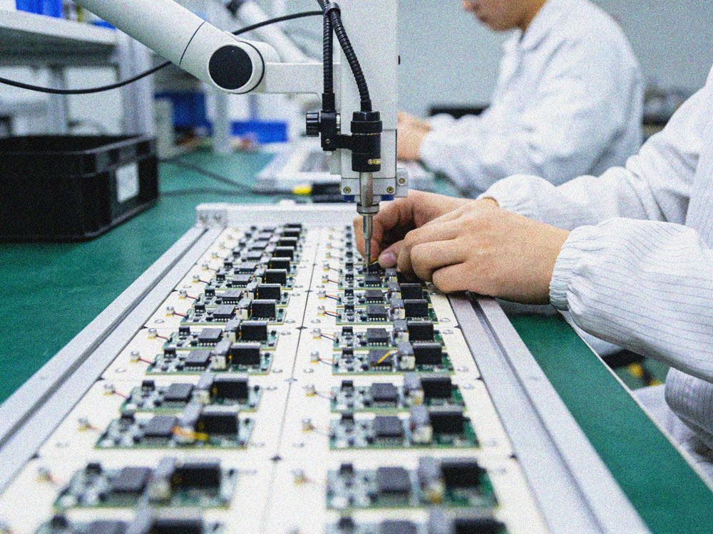
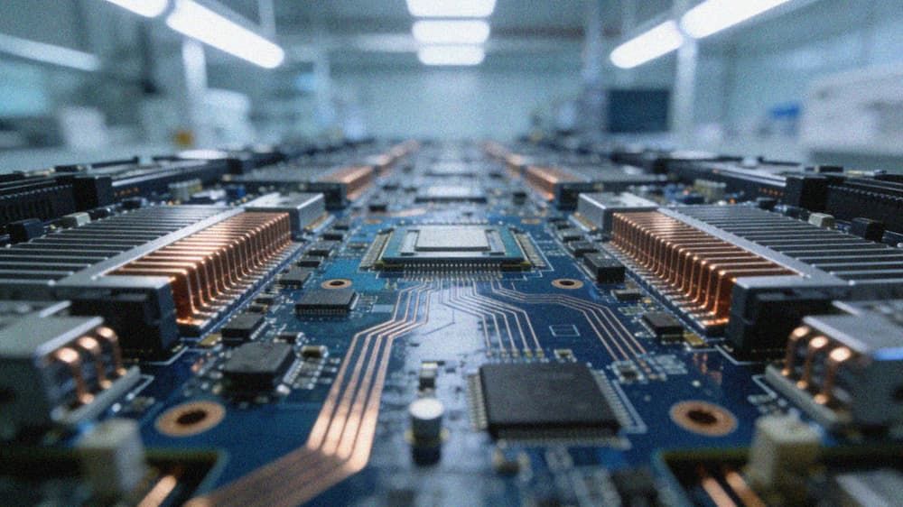
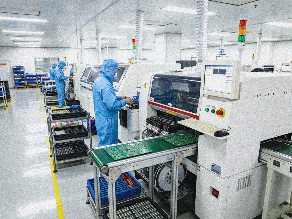
Driven by the powerful computing demands of artificial intelligence, server hardware is undergoing a profound transformation. As the core carrier of GPUs, high-speed CPUs, and complex interconnects, the design and manufacturing complexity of AI server motherboards (PCBs) has increased dramatically. Traditional multilayer board technology is no longer sufficient to meet the signal integrity, power integrity, and heat dissipation requirements of high-computing power, high-bandwidth, and high-power consumption scenarios. Therefore, breaking through the technical bottleneck of 20-40 layer high-density interconnect (HDI) PCBs has become a key battleground that AI server PCB manufacturers and AI data center PCB manufacturers must conquer.
This technological breakthrough is not a single-stage improvement, but a systematic project spanning materials science, precision machining, simulation design, and reliability verification. Based on over 27 years of R&D and manufacturing experience in the field of high-speed, high-multilayer PCBs, we have outlined the breakthrough paths for several core bottlenecks as follows.
The Ultimate Challenge of Layer Count and Density
AI server motherboards need to integrate massive amounts of data processing units and high-speed interfaces, directly requiring PCBs with extremely high wiring density and more signal layers. According to technical parameters in the knowledge base, typical multi-layer products for AI computing servers have 16-32 layers, while our prototype manufacturing capabilities can even push the number of layers in FR4 material to 72 layers, with mass production capabilities reaching 32 layers. This provides ample wiring space for complex AI hardware.
However, increasing the number of layers is only the foundation; the real challenge lies in achieving high-density interconnects within a limited thickness. This requires extreme control over line width and spacing. In our AI server motherboard products, the line width and spacing at the CAM (Computer-Aided Manufacturing) level has reached 4.5/2.5 mil (approximately 114/64 micrometers). In the more advanced HDI and Substrate-Like PCB (SLP) fields, the line width/spacing capability at the prototype stage can reach 25/25 micrometers. This precision ensures that tens of thousands of high-speed differential signal lines can be laid out in a 20-40 layer stack-up, providing physical channels between the GPU and High Bandwidth Memory (HBM), as well as high-speed interfaces such as PCIe 5.0/6.0.
The "Invisible Killer" of High-Speed Signal Integrity
As signal rates move towards 112Gbps (prototype stage) and even higher, any tiny impedance deviation, reflection, or crosstalk can lead to system failure. This places millimeter- to micrometer-level precision requirements on the design and manufacturing of HDI PCBs.
First, impedance control is the lifeline. Multiple case studies in the knowledge base show that in products such as high-speed backplanes and optical modules, impedance tolerances are strictly controlled within ±5% (prototype) to ±8% (mass production). Achieving this goal relies on precise layer stack-up design, high-speed materials with stable dielectric constants (such as TU933+, Panasonic M6/M7N), and a deep understanding of etching factors. For example, in the manufacturing of millimeter-wave radar PCBs, antenna etching accuracy needs to be controlled within ±0.5 mil, and this also applies to critical high-speed networks in AI motherboards.
Secondly, reducing the "stub effect" in signal transmission is crucial. Back drilling technology has become standard practice. Our technology portfolio explicitly includes "multiple back drilling" capabilities, which precisely control the drilling depth to remove unused copper pillars in vias, thereby reducing signal reflection and attenuation. This is particularly critical for improving signal quality in high-speed backplanes up to 5.5mm long and 26 layers (with an aspect ratio of 25:1).
Finally, a closed loop of pre-design simulation and post-design manufacturability (DFM) is indispensable. We utilize our self-developed KBEDA SKILL tool (based on the Cadence platform, integrating over 400 functions) for signal integrity (SI) and power integrity (PI) simulations. In the Jetson AGX Xavier evaluation board project, the team pre-optimized the routing of the 100-ohm differential impedance through simulation and utilized four ground planes in the 10-layer board to provide low-impedance return paths, effectively managing the signal integrity challenges brought by 750Gbps high-speed I/O.
The "Thermal Game" of Power Delivery and Thermal Management
AI accelerator cards and server CPUs often consume hundreds of watts, with huge instantaneous currents. This requires the PCB's power distribution network (PDN) to have extremely low impedance and strong current-carrying capacity. Simultaneously, the enormous heat must be efficiently dissipated; otherwise, high temperatures will lead to material performance degradation and signal distortion.
In terms of power supply, thick copper technology is fundamental. Our technical capabilities show that the maximum copper thickness can reach 18 OZ (prototype), with mass production at 6 OZ. In high-current products such as new energy vehicle motor drive modules, even 4-6 OZ finished copper thickness combined with aluminum-based hybrid voltage technology is used to cope with the extreme current of 330A. For AI motherboards, using 2oz or 3oz thick copper for the power layer is a common design to ensure that voltage drop (IR drop) is within acceptable limits during instantaneous loading.
Thermal management is a comprehensive test of materials and processes. Besides using high thermal conductivity substrates (such as high thermal conductivity PP, 2.0W/mk) and thermally conductive adhesive films, a special heat dissipation structure design is crucial. For example, in copper-based products with thermoelectric separation bumps, single-sided bumps are formed by etching windows combined with laser depth control technology, directly dissipating the chip's heat points through the copper bumps, with bump height tolerance controlled within ±25 micrometers. This approach can also be applied to areas of high heat flux density in AI server motherboards. Furthermore, "precision control technology for metallized slots and crimp holes" not only meets the needs of special connectors, but its precise metallized holes also help establish vertical heat dissipation paths.
The Technological Gap Between High Aspect Ratio Manufacturing and Microvia Interconnects
20-40 layer boards mean a board thickness that may exceed 3.2mm, and to maintain high density, the aperture must be as small as possible. This creates a huge aspect ratio (board thickness/aperture). Knowledge base data shows that for through-holes, the maximum aspect ratio capability is 25:1 (prototype), and 16:1 in mass production. This means that to stably electroplate a deep hole with a diameter of only 0.16mm on a 4.0mm thick board, and ensure uniform and reliable copper penetration, poses a severe challenge to both drilling and electroplating processes. We address this through high aspect ratio board drilling technology and pulse electroplating technology.
For even greater space savings, HDI technology must be introduced. Blind vias, stacked vias, and staggered via designs can significantly reduce the number of through-holes, freeing up wiring space. In the "AI Accelerator Card HDI Board with Stacked Vias" case, a two-tier stacked via + mechanical blind via design was adopted, and "BGA laser filling + resin pad in-hole processing technology" was applied, ensuring surface flatness while increasing density. In the "11-tier staggered via HDI Board," 10-14 tiers of staggered via interconnection were achieved, with line width and spacing of 0.075/0.075mm, demonstrating the ability to handle extreme high-density requirements in the industrial control equipment field. Its "advanced HDI expansion and contraction control technology" is also of reference value for AI server motherboards.
Systematic Capability is the Ultimate Barrier
In summary, breaking through the bottleneck of 20-40 layer high-density PCBs is far more complex than simply purchasing a few advanced devices. This requires AI server PCB manufacturers to possess a complete, systematic capability across the entire chain, from material selection (such as TU933+ high-speed materials), precision manufacturing processes (such as 4.5/2.5mil linewidth and spacing, 0.2mm minimum hole diameter, and multiple back-drilling), to simulation design (SI/PI) and reliability verification (such as high and low temperature cycling and vibration testing).
Ultimately, the results of these technological breakthroughs will be tangibly reflected in products: an AI server motherboard capable of stably handling kilowatt-level power consumption, supporting hundreds of gigabits per second of data throughput, and operating continuously 24/7 in harsh data center environments. For AI data center PCB manufacturers, this ability to transform abstract technical parameters into highly reliable hardware entities is the core competitiveness that empowers the next generation of AI computing infrastructure. This technological battle surrounding density, speed, and heat is ongoing, and every solid breakthrough in manufacturing processes lays a more robust physical foundation for the leap in computing power for artificial intelligence.