In the context of the widespread application of 800V high-voltage platforms and SiC inverters, power electronics PCB design is facing unprecedented challenges. As power density continues to increase, traditional layout solutions often lead to problems such as large signal interference, low acquisition accuracy, and excessive PCB temperature rise, thereby shortening product life. Especially in the field of Automotive electronics PCB design, high-voltage safety and thermal runaway protection must be given top priority. It has become an industry consensus to achieve fast heat dissipation and high power density by optimizing circuit design to meet the 330A limit current and high temperature and high heat dissipation requirements. This article will dismantle 5 core layout techniques that can significantly improve system efficiency based on actual engineering cases.
1. High-voltage isolation and stacked architecture optimization
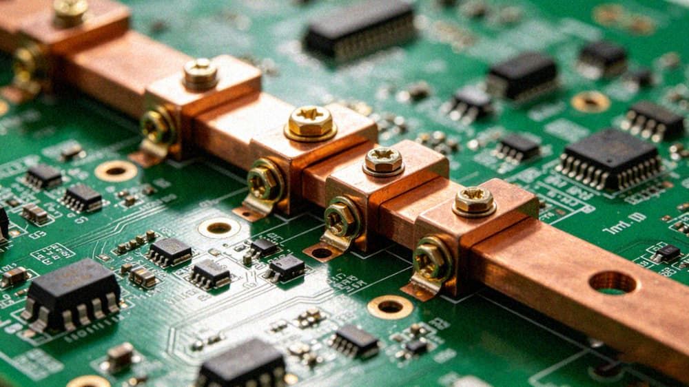
In high-voltage scenarios such as ±350V converter valves and ±400V cabinet power distribution, the isolation design layout of high-voltage and low-voltage is the basis for ensuring functional safety. Traditional single-layer or double-layer board designs are difficult to meet strict insulation and voltage requirements. It adopts a four-layer board layered design (signal/ground/power/shielding layer) to isolate the high and low voltage areas, and embeds copper-based heat sinks to reduce thermal resistance. This is a proven and effective solution. This architecture not only optimizes the impedance matching and filtering circuit (π filter + common mode inductor), but also integrates self-diagnostic pins to quickly locate faults.
High Voltage Design Checklist
| Parameter items | Specification requirements | Remarks |
|---|
| Voltage level | ±350V converter valve / ±400V cabinet power distribution | Set according to application scenario |
| Stacked structure | Signal/ground/power/shielding layer | Four-layer board layered design |
| Insulation isolation | Physical isolation of high-voltage and low-voltage areas | Preventing the risk of breakdown |
| Process requirements | High reliability surface treatment (immersion gold/immersion tin) | Improve corrosion resistance |
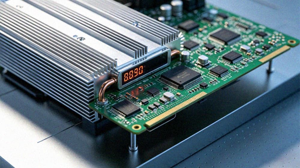
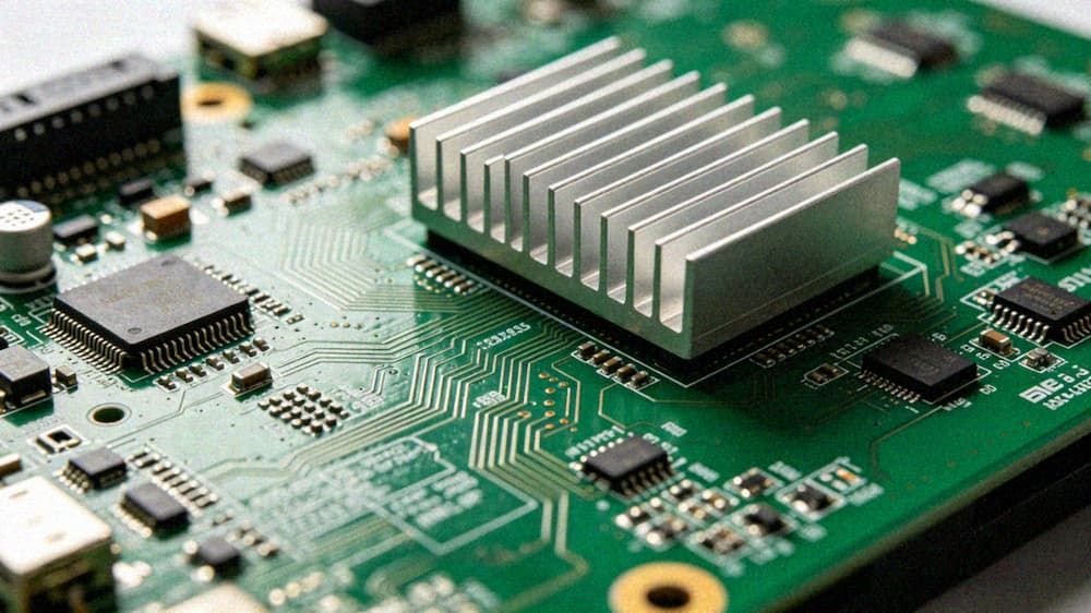
2. Large current carrying and superconducting thermal design
The heat dissipation and high current carrying issues of high-power power equipment directly determine the yield rate of PCB Design & Manufacturing. In order to meet the 330A limit current, the key is to use ≥5OZ thick copper core board, 2W high thermal conductivity PP and aluminum-based mixed voltage technology. The wiring layout for ultra-high current needs to be combined with the surface lamination board manufacturing process of large copper strips with high thermal conductivity to ensure current carrying capacity.
Current Carrying Capacity Table
| Copper thickness specifications | Line width recommendations | Continuous current carrying | Temperature rise control |
|---|
| ≥5OZ thick copper | Calculated based on impedance | Meet 330A limit current | High temperature and high heat dissipation requirements |
| More than 2oz copper thickness | Optimize solder paste volume | Avoid virtual soldering or pad peeling | Optimize reflow soldering temperature profile |
| Embedded copper block | Local enhancement | High power density areas | Reduce thermal resistance |
3. Signal integrity and EMC filter layout
Large signal interference often leads to low acquisition accuracy. In PCB Design, reasonable wiring design (such as differential pair wiring, impedance matching) reduces signal interference and reflection and ensures the stability of signal transmission. Optimized impedance matching and filter circuit (π filter + common mode inductor) can effectively suppress conductive electromagnetic interference and radiated electromagnetic interference generated by high current and high voltage switching circuits. For RF PCB Design, the integrity of the shielding layer is also critical.
4. Precision component layout and DFM manufacturability
With the miniaturization of components, the precise placement of micro components such as 0402 and 0201 has become difficult. Using high-precision placement machines to ensure the reliability of 0201 (0.6mm0.3mm) or even 01005 (0.3mm0.2mm) packages is one of the core capabilities of PCB Design Service. DFM approved the layout for a compact design, and the finished product is suitable for recessed installation. The minimum PIN spacing needs to be controlled at 0.35mm, and the device height must meet the double-sided process requirements (≤25mm).
5. Material selection and rigid-flex technology
Preferred substrate materials are usually thick copper, multi-layer high-grade, and aluminum substrates. FR-4 high TG material, polyimide (PI) or ceramic substrate to meet stability requirements in high temperature and high humidity environments. Flexible PCB Design and rigid-flex board technology (such as rigid-flex board with gold finger reinforcement) have obvious advantages in space-constrained scenarios. Through heat dissipation + material + process optimization, create a highly stable power industry PCB.
Comparison of Thermal Management Solutions
| Heat dissipation solution | Thermal resistance characteristics | Cost | Complexity | Applicable scenarios |
|---|
| Embedded copper heat sink | Low thermal resistance | Medium | Medium | High power density module |
| Aluminum-based hybrid voltage technology | High thermal conductivity | Low | Low | Universal power strip |
| Ceramic substrate | Extremely low thermal resistance | High | High | Extremely high temperature environments |
| 2W high thermal conductivity PP | Optimized heat conduction | Medium | Medium | Multilayer board internal heat dissipation |
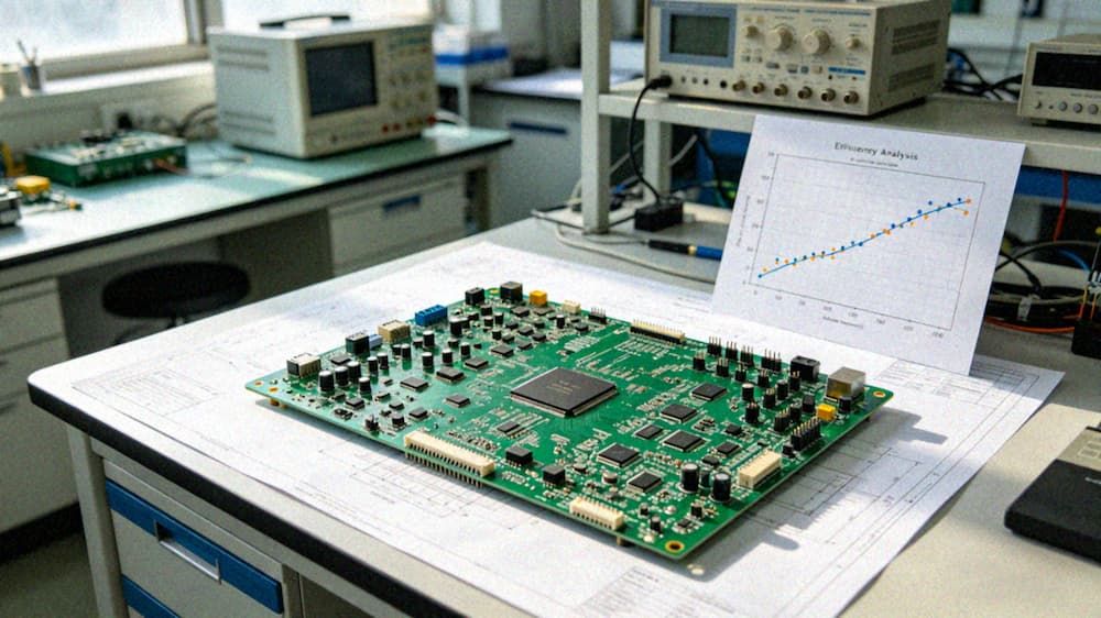
Case verification and data closed loop
In a certain high and low voltage power supply measurement board (IPM solution) project, the purchasable product BOM was obtained through reverse engineering of the product. The standard parts materials were strictly based on the original factory specifications and model descriptions. After implementing the above layout techniques, the quantitative data of the solution value show that the overall performance of the board is improved by 99%, the yield rate is increased to 100%, and the cost is reduced by 10%. In the case of Automotive PCB Design, the inverter drive board and motor drive board achieved full digital implementation of DSP and automatic over-temperature derating protection through carefully selected automotive-standard component services and precise welding process services.
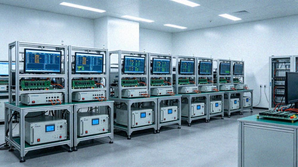
In addition, Zhilian Testing conducted high and low temperature cycle and vibration tests on the board to verify the product's operational stability in extreme environments. For the design of power boards with copper thickness of more than 2oz, optimize the solder paste volume and reflow soldering temperature curve to avoid false soldering. PLM system components are optimized to reduce component procurement costs and shorten delivery times. These measures work together to solve the core pain points of single charging mode and high energy consumption of AC inverter, and significantly improve the problem of slow energy efficiency conversion of high-voltage DC charging.
To sum up, Power Electronics PCB Design is not only the realization of electrical connections, but also the coupling optimization of electrical-thermal-magnetic-mechanical multi-physical fields. By following the high-voltage safety priority narrative, combining specific vertical scenario cases, and mapping general technologies to specific applications, the reliability of the system in 800V high-voltage platforms and SiC inverter applications can be ensured. From signal integrity control to anti-corrosion surface treatment process, refined control of every link is the key to improving final efficiency.