Overview
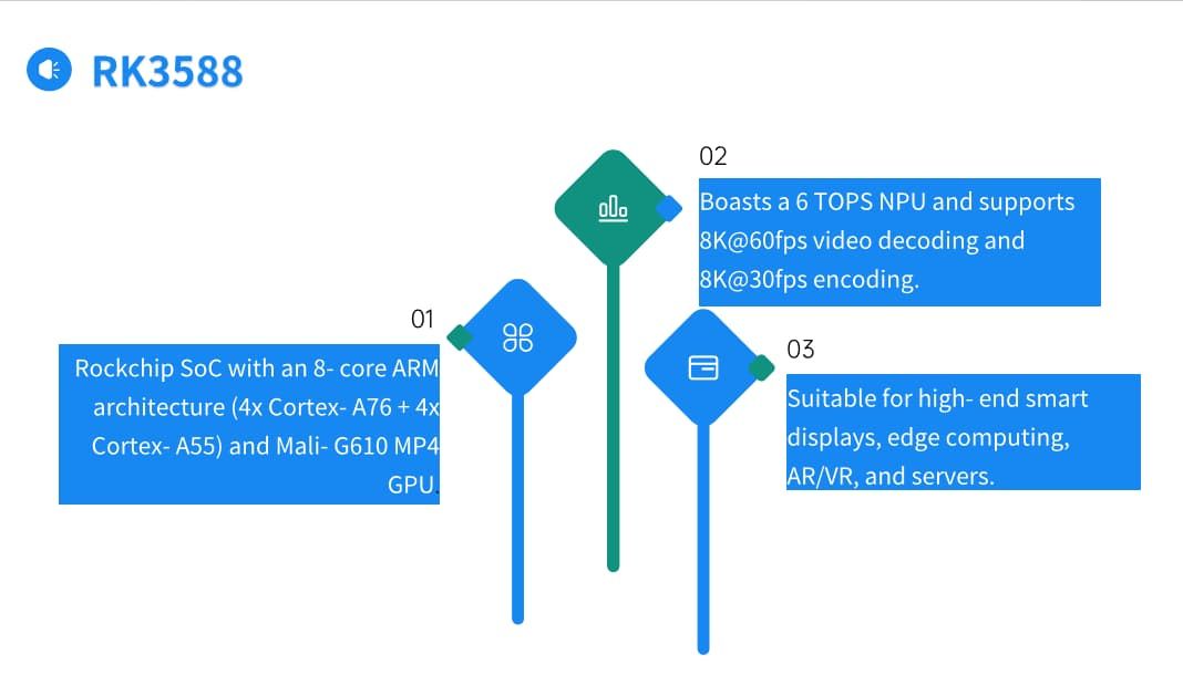
AI edge devices are core carriers for realizing low-latency computing, on-site data processing, and intelligent response in distributed AI deployment scenarios, covering consumer smart terminals, industrial intelligent equipment, smart city nodes, and automotive edge electronics. Unlike cloud computing hardware, edge AI devices have strict requirements for PCB miniaturization, heat dissipation performance, signal transmission stability, and environmental adaptability, to adapt to harsh deployment conditions such as limited space, variable temperatures, and long-term unattended operation. Professional AI edge device PCB suppliers provide full-process solutions covering design optimization, prototyping, small-batch trial production, and large-scale mass production, addressing core pain points such as high-speed signal attenuation, thermal runaway of high-computing chips, and rigid-flex integration constraints, to support the stable operation of 16TOPS+ high-performance edge AI hardware.
Technical Capabilities
AI edge device PCB suppliers have mature manufacturing processes and customized technical systems to meet the diversified needs of different edge AI application scenarios:
- Full Product Type Coverage: Support manufacturing of single and double-sided boards, 2-40 layer high-speed multilayer boards, HDI boards, rigid-flex boards (including buried via design, gold finger reinforced types), high-frequency hybrid boards, heavy copper boards, high-speed backplanes, embedded component boards, metal core substrate boards, and high heat dissipation ceramic boards, with no minimum order quantity restrictions, adaptable to R&D verification, small batch trial production, and large-scale mass production needs.
- High-Speed Transmission Support: Enable up to 750Gbps high-speed I/O transmission performance, with ±5% high-precision impedance control for 90Ω/100Ω differential signals, and support stack design with up to 6 independent ground planes, effectively shielding signal crosstalk between layers, reducing signal reflection and attenuation, and adapting to the transmission requirements of high-computing GPUs, FPGAs, and dedicated edge AI SoC chips.
- High-Density Integration Process: Support micro-via processing down to 0.06mm, line width/line spacing as small as 2.0/2.0mil, and embedded capacitor, embedded resistor, and embedded component manufacturing processes, meeting the miniaturization and lightweight design requirements of portable edge AI terminals such as IoT handheld devices and intelligent wearable equipment.
- Thermal Performance Optimization: Provide a variety of high thermal conductivity substrate options including metal core substrates, buried ceramic substrates, and thick copper boards, with thermal conductivity up to 15W/m·K, effectively dissipating heat generated by high-load edge computing chips, ensuring stable operation of equipment under long-term full-load working conditions.
- Value-Added Full-Chain Services: Provide pre-design services including schematic review, stack planning, and signal integrity simulation, as well as BOM optimization, component sourcing and management, and PCBA assembly support, reducing cross-stage communication costs and shortening the product R&D cycle by 30% on average.
Quality Standards
AI edge device PCB suppliers follow strict quality control systems throughout the design and manufacturing process to ensure product reliability in complex edge deployment scenarios:
- Industry Compliance Alignment: Production processes fully comply with ISO 9001, IATF 16949, ISO 13485 and other industry-specific quality management system requirements, and testing links are accredited to ISO/IEC 17025 standards, meeting the access requirements of industrial, automotive, medical, and communication edge AI application scenarios.
- Full-Process Testing and Verification: Equipped with professional testing laboratories, providing signal integrity testing, EMC testing, thermal cycle testing, high and low temperature impact testing, vibration testing, and salt spray testing, ensuring products operate stably in the industrial temperature range of -40℃ to +85℃, and adapt to harsh environments such as high humidity, dust, and frequent vibration.
- High Yield Control Mechanism: Adopt advanced production equipment including laser drilling, LDI laser direct imaging, and X-Ray non-destructive testing, with 100% online inspection coverage for key processes, achieving over 98% yield for high-complexity high-speed multilayer boards and HDI boards, reducing unnecessary production costs for customers.
Applications
Specialized PCB solutions provided by AI edge device PCB suppliers are widely applicable to various edge AI hardware scenarios, including but not limited to:
- Industrial Edge Intelligence: Industrial robot master control boards, mechanical arm control boards, ATE equipment test boards, intelligent inspection terminal boards, industrial edge computing node boards, and thyristor control unit boards
- Consumer Smart Terminals: Smart audio mainboards, smart home appliance control boards, IoT handheld device boards, face recognition terminal boards, and intelligent logistics terminal boards
- Smart City Edge Nodes: Intelligent environmental monitoring terminal boards, security monitoring mainboards, traffic edge computing unit boards, 5G edge gateway boards, and community intelligent service terminal boards
- Automotive Edge Electronics: Autonomous driving domain controller boards, smart cockpit core control boards, vehicle edge computing platform boards, and in-vehicle perception system interface boards
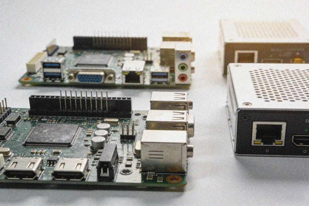
- High-Performance Edge Computing Hardware: GPU/FPGA high-performance computing cards, optical module boards, 16TOPS+ AI core boards, dedicated edge SoC supporting boards, and high-frequency 5G antenna boards
Key Advantages
Compared with general PCB manufacturers, AI edge device PCB suppliers have obvious professional advantages in meeting the special needs of edge AI scenarios:
- Scenario-based Customization Capability: Adjust PCB material selection, stack design, and process route according to the actual deployment environment of edge AI devices, providing targeted solutions for low-power portable terminals, high-computing industrial edge nodes, and vehicle-mounted high-reliability equipment.
- Full Lifecycle Production Support: Cover all production stages from R&D prototyping, small batch trial production to large-scale mass production, with no minimum order quantity restrictions, meeting the flexible production needs of different R&D and commercial operation stages.
- Mature Project Implementation Experience: Have rich practical experience in high-complexity edge AI PCB projects, including 16Tops high-computing core boards, rigid-flex handheld IoT terminals, and industrial high-heat dissipation robot control boards, with mature and reliable solutions that can effectively avoid design and manufacturing risks.
- Cost and Efficiency Optimization: Integrate design, manufacturing, and supply chain services, reduce redundant communication links, and balance product performance and manufacturing cost through pre-design feasibility review and BOM optimization, helping customers improve product market competitiveness.
Contact Information
If you have customized PCB requirements for AI edge devices, including prototyping, small batch trial production, or large-scale mass manufacturing demands, you can contact our professional technical team for support. We will provide you with free pre-sales technical evaluation, customized solution design, and transparent quotation services to help your edge AI product R&D and commercial landing go smoothly.