Overview
Energy monitoring systems are core infrastructure for smart grid operations, industrial energy efficiency optimization, and renewable energy deployment, requiring printed circuit boards that deliver consistent sensing accuracy, high heat dissipation capacity, and long-term reliability in volatile electrical and environmental conditions. Poorly optimized PCBs for energy monitoring use cases can lead to inaccurate current/voltage data collection, premature component failure, and non-compliance with industry safety standards, directly undermining the performance of energy management infrastructure. Energy monitoring PCB manufacturers offer end-to-end custom PCB design, manufacturing, and testing solutions tailored to the unique requirements of energy monitoring hardware, addressing core pain points such as high-voltage isolation, electromagnetic interference (EMI) resistance, and stable operation across wide temperature ranges. Solutions cover both low-power compact sensing modules and high-power high-voltage grid monitoring units, supporting all project stages from early R&D prototyping to full-scale mass production.
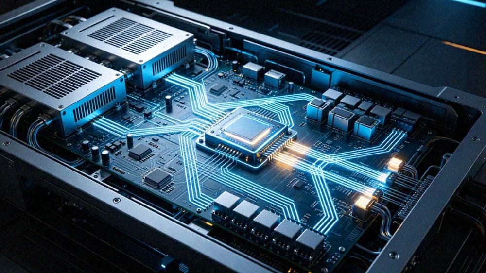
Technical Capabilities
- Diverse PCB Product Type Support: Manufacturers support production of a full range of PCB types suitable for energy monitoring use cases, including single and double sided boards, 2-32 layer multilayer boards, HDI boards, heavy copper (up to 12oz copper thickness) boards, high-frequency hybrid boards, rigid-flex and semi-flexible boards, metal core and metal substrate boards, high-speed backboards, and embedded capacitor/resistor/component boards. This broad product portfolio covers all functional requirements for energy monitoring hardware, from low-power wireless communication modules to high-power load monitoring circuits.
- Flexible Dimensional & Assembly Adaptability: Production lines support both standard and unconventional PCB sizes, with maximum board dimensions of up to 600mm x 450mm for semi-automatic printing compatible designs. Assembly capabilities support component thickness ranging from less than 0.5mm to over 3mm, minimum pitch accuracy of 0.5, and support for ultra-small component packages as small as 01005 (0.3mm x 0.2mm) for compact portable energy monitoring devices. Double-sided assembly supports component heights up to 25mm, with maximum SMD component sizes of up to 200mm x 125mm for high-power monitoring unit designs.
- High-Precision Performance Optimization: Manufacturers deliver tight impedance control (±5% tolerance) for high-speed signal transmission paths, ensuring accurate sensing data transmission from current/voltage sensors to processing units without signal attenuation or crosstalk. High-frequency material options support stable wireless data transmission for IoT-enabled energy monitoring terminals, while thick copper constructions ensure efficient heat dissipation for high-voltage, high-current monitoring circuits, reducing thermal stress on components and extending product lifespan.
- No Minimum Order Quantity (MOQ) Support: Flexible production scheduling supports both low-volume prototyping runs for R&D verification and high-volume mass production for commercial deployment, with no mandatory minimum order quantity requirements for all supported PCB types. This allows hardware developers to test design iterations at low cost before scaling to full production, reducing overall project risk and upfront investment.
Quality Standards
All energy monitoring PCBs are manufactured in compliance with global industry quality and safety standards, with production processes certified under ISO 9001 quality management systems, IATF 16949 for automotive-grade energy monitoring hardware, and ISO 13485 for medical energy monitoring applications. Testing facilities are accredited under ISO/IEC 17025, with mandatory full-process testing for all production runs, including signal integrity testing to verify sensing data accuracy, EMC/EMI testing to ensure compliance with grid electromagnetic interference requirements, high and low temperature cycling testing (-40℃ to +85℃), humidity resistance testing, voltage withstand testing, and thermal shock testing to validate performance in harsh field operating conditions. All finished products undergo 100% electrical performance testing before shipment, ensuring zero defective rates for mass production runs.
Applications
Energy monitoring PCB solutions are widely deployed across a range of energy management use cases, including:
- Smart Grid Monitoring Terminals: Heavy copper and metal substrate PCBs for high-voltage distribution grid monitoring units, supporting stable operation in high-electromagnetic interference grid environments
- Residential & Commercial Smart Energy Meters: Compact single/double sided and multilayer PCBs for low-power smart meters, with optimized low-power signal paths to extend battery lifespan for off-grid metering deployments
- Solar PV & Wind Energy Monitoring Systems: High-frequency and rigid-flex PCBs for renewable energy generation monitoring modules, with high weather resistance to support outdoor deployment in extreme temperature and humidity conditions
- Industrial Power Consumption Monitoring Equipment: Thick copper multilayer PCBs for industrial factory energy management systems, supporting high-current load monitoring and high-speed data transmission to central control platforms
- Electric Vehicle (EV) Charging Pile Monitoring Units: Rigid-flex and metal core PCBs for EV charging pile power and data monitoring modules, with high heat dissipation capacity to support continuous high-power charging operations
- Battery Energy Storage System (BESS) Monitoring Modules: High-density HDI and embedded component PCBs for BESS state of charge (SOC) and state of health (SOH) monitoring units, ensuring accurate real-time battery performance data collection
- Building Energy Management System (BEMS) Control Boards: Multilayer high-speed backboards for commercial building energy management control units, supporting integration of multiple sensing and control circuits for whole-building energy optimization
Key Advantages
- Scenario-Specific Customization: Manufacturers work closely with hardware development teams to optimize PCB designs for specific use case requirements, including material selection, stackup architecture, copper thickness, and impedance matching, ensuring that the final product meets performance, cost, and form factor targets.
- Full Lifecycle Technical Support: Technical teams provide end-to-end support from early design feasibility evaluation, DFM (design for manufacturing) optimization, prototyping testing, to mass production quality control, reducing cross-stage communication friction and shortening time to market for new energy monitoring products.
- High Yield & Cost Efficiency: Advanced production equipment including laser drilling, LDI laser direct imaging, and X-Ray non-destructive testing ensure high manufacturing yield rates (over 98% for standard designs), reducing overall production costs and minimizing waste for mass production runs.
- Long-Term Reliability Guarantee: All PCBs are designed and tested to meet a minimum service life of 10 years for static indoor deployments and 5 years for outdoor field deployments, with performance warranties covering material defects and manufacturing faults for all production runs.
Contact Information
If you have custom requirements for energy monitoring PCBs, reach out to our technical support team for a free, no-obligation project evaluation and customized solution quotation. Our engineering experts will provide professional guidance on material selection, stackup design, manufacturing feasibility, and compliance testing to help you bring high-reliability, high-performance energy monitoring products to market efficiently.