SEO Description: Focusing on the design requirements of the ai robot control system pcb, analyze the design points of HDI, rigid-flexible combination, thick copper, EMC and DFM in the AI robot perception layer, decision layer, execution layer and inter-board communication to help the hardware team identify PCB engineering risks before mass production.
Body
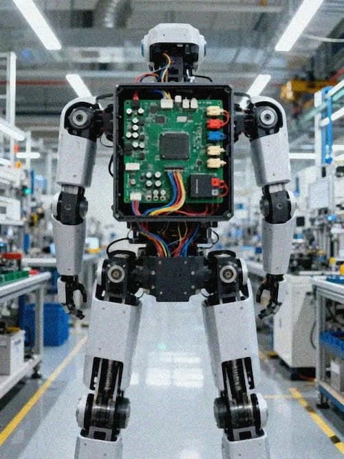
An AI Robot Control System usually consists of a Perception Layer, a Decision Layer, and an Action Layer. The sensing layer is connected to cameras, lidar, IMU, force sensing sensors and other devices, and is responsible for transforming the external environment and its own posture into computable data; the decision-making layer runs computing chips such as CPU, GPU, and NPU to complete visual understanding, path planning and Action generation; the execution layer converts control instructions into motor drive, current regulation, and joint movement. The difficulty in designing the ai robot control system pcb around these three layers lies in the simultaneous appearance of high-speed signals, miniaturized wiring, high current carrying and anti-interference requirements within the same machine. The value of HDI PCB technology goes beyond making the board smaller. It provides a system-level routing method that integrates high-density interconnections, stack planning, thermal paths and manufacturing consistency in the same engineering diagram.
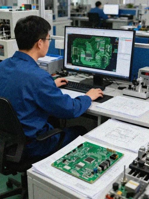
During the prototype stage, the robot hardware team often pays more attention to whether the algorithm passes, whether the sensors are available, and whether the joints can move stably. After entering the small batch and mass production stage, the problem will turn to the PCB level: whether the main control board can complete high-speed storage and multiple sensor access within a limited area, whether the sensing board in the head or joints can withstand bending and vibration, Whether the drive board will experience local temperature rise under peak current, and whether the connection between the boards remains stable when the whole machine is moving. Since these problems are usually not fully exposed when the single board is lit up, but appear after joint debugging of the whole machine, EMC testing, thermal cycling or long-term operation, PCB design needs to be involved in architecture review at an earlier stage. For robot control systems, reasonable HDI design should be involved at the architecture stage, which determines the starting point for manufacturability and long-term reliability of the whole machine.
Decision Layer PCB: Edge AI computing power pushes HDI to higher levels
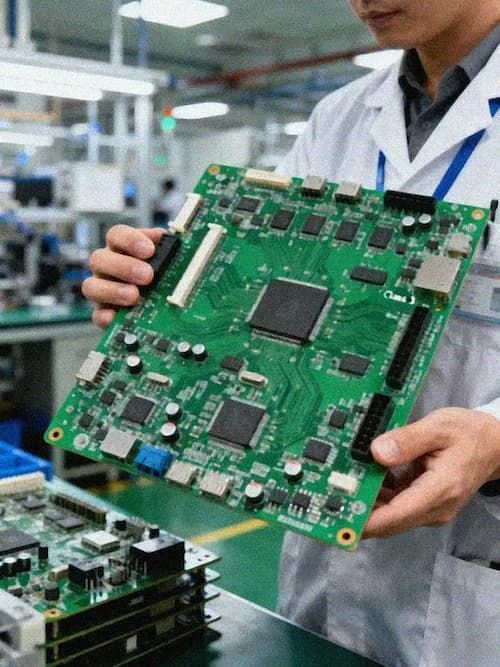
The decision-making layer undertakes the centralized computing tasks of the robot and usually integrates CPU, GPU, NPU, LPDDR, eMMC or NVMe storage, as well as Ethernet, MIPI, USB, PCIe and other interfaces. Taking edge AI chips such as RK3588 as an example, 6TOPS-level NPU can already support multi-channel Media Processing Service and local reasoning, and is suitable for robot control, industrial vision and edge AI devices. The PCB space of this type of main control board is not abundant, because the robot's head, trunk or control box also needs to accommodate heat sinks, wiring harnesses, battery management modules and structural parts. BGA spacing, DDR trace length matching, high-speed differential pair return path and power integrity of chip packages need to be processed simultaneously within a limited board area.
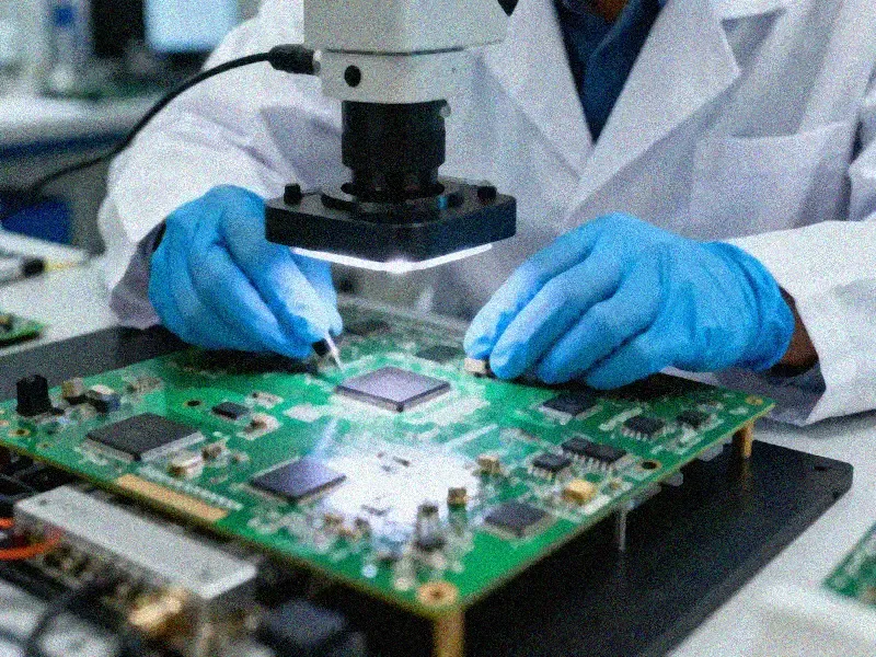
High-level HDI is a common solution path for decision-level PCBs. Server and AI computing power motherboards have pushed high-level multilayer manufacturing to the level of 32-layer mass production and 56-layer sample verification. Robot main control boards usually do not reach the number of layers of server motherboards, but 12 to 20-layer HDI stacks are becoming common. 0.2mm laser microvias can shorten the inter-layer interconnection path, reduce the occupation of inner layer wiring channels by traditional vias, and also facilitate BGA wire escape and power plane continuity. Kingbrother's process accumulation in high-multilayer boards, HDI arbitrary layer interconnections and 0.2mm laser drilling is suitable for early DFM evaluation of such high-density main control boards, especially in complex chip packaging, large number of interfaces, and tight board space.
Risk at the decision-making level is concentrated at the junction of signal integrity and thermal management. DDR5 can reach 6400MT/s, LPDDR5X can reach 8533MT/s, and MIPI and PCIe links will also push wiring length, impedance control, reference plane and via stubs to stricter limits. At the same time, the power consumption of high-computing chips may reach 15 to 60W, which is lower than that of the server GPU, but is enough to create a continuous thermal load within the small robot shell. If the stack is only planned according to wiring density, thermal vias, heat dissipation pads and copper planes are not designed in advance, and adding heat sinks or air ducts later often only reduces the surface temperature and cannot solve the local thermal resistance under the chip. The design of the main control board needs to incorporate impedance, return path, power integrity and thermal diffusion into the simulation at the same time, rather than waiting for the model to come back and then relying on experience to repair it.
A typical engineering scenario is where the team selects high-performance NPU modules during the prototype stage, and the initial PCB uses fewer layers and relatively conservative line widths and spacing in order to shorten the development cycle. During single-board debugging, the camera, IMU and motor control link can all work normally; after the whole machine is running continuously for several hours, the visual inference frame rate begins to fluctuate, and sporadic MIPI errors and power ripple appear at the same time. Subsequent investigation found that DDR traces around the NPU passed through discontinuous reference planes, and the copper distribution in the power layer was affected by connectors and mounting holes. Local temperature rises caused the superposition of impedance and power supply noise. The engineering team finally solved the problem by adding stacks, adjusting the BGA escape method, strengthening the power plane and rearranging the thermal via array. Such cases illustrate that the HDI design of decision-level PCBs needs to be involved in the architecture stage to avoid passively accepting packaging, heat dissipation and interface constraints during the routing stage.
Sensing layer PCB: The spatial constraints of sensor fusion boards are closer to manufacturing issues
The sensing layer PCB is usually distributed near the head, chest, wrist, foot or joints, and is responsible for multi-channel sensor access and preliminary signal sorting. Camera modules require MIPI CSI-2, lidar and depth cameras may require high-speed serial interfaces, and IMUs and force sensors are more sensitive to analog noise and ground-bomb noise. Space constraints are the most direct engineering constraint for such boards, because structural design often leaves PCB with shaped areas, curved spaces, or narrow cavities close to moving parts. Industrial robots can use relatively regular control cabinets, while humanoid robots and collaborative robots have difficulty leaving loose wiring space for sensor boards.
Any layer interconnected HDI and rigid-flexible board have high application value in the sensing layer. Micro-blind holes reduce the area occupied by through-holes, buried holes allow the internal signal layer to maintain a more complete wiring channel, and rigid-flexible bonding plates can disperse sensors, connectors and main chips on different structural surfaces. A typical head sensor board may use 4 to 8 layers of HDI lamination, 0.1mm line width and line spacing, 0.15mm micro blind holes, and carry multiple MIPI CSI-2 four-channel links. Since the rate per channel can reach 2.5Gbps, differential impedance, line length matching and reference plane continuity still need to be strictly controlled. Even if the board area is small, it cannot be handled as an ordinary small signal board.
Another difficulty in the sensing layer comes from noise coupling. High-speed camera data, IMU low-noise power supply, weak analog signals from force sensors, and motor switching noise near joints are often compressed in the same small area. If the ground plane division is not handled properly, digital return current may be directed near the analog sensor; if the connector layout only considers assembly convenience, the movement of the wiring harness will transfer mechanical stress to the solder joints and flexible areas; when the bending radius of the flexible section is insufficient, copper foil fatigue will appear as intermittent open circuits after long-term exercise. For AI robot HDI boards, miniaturization is only a superficial result. What is more difficult to control is the common boundaries of signal, mechanical and manufacturing tolerances.
Kingbrother's rigid-flexible composite board, HDI blind hole buried hole and arbitrary layer interconnection capabilities are suitable for participating in stacking and structural review early in the sensing layer design. For head sensor boards, the connector direction, flexible zone bending path, sensor relative position and assembly tolerance should be confirmed before the ID design is completed; for sensor boards near the joints, it is also necessary to incorporate vibration, impact and repeated bending into the weld joint fatigue into reliability verification. Many sensing board failures do not come from wrong circuit principles. The root causes are often structural space, connector stress and PCB process windows not aligned in advance. Early DFM reviews can help teams move these issues forward from the complete machine testing phase to the prototype phase.
Execution layer PCB: The joint driver board must handle both high current and EMC
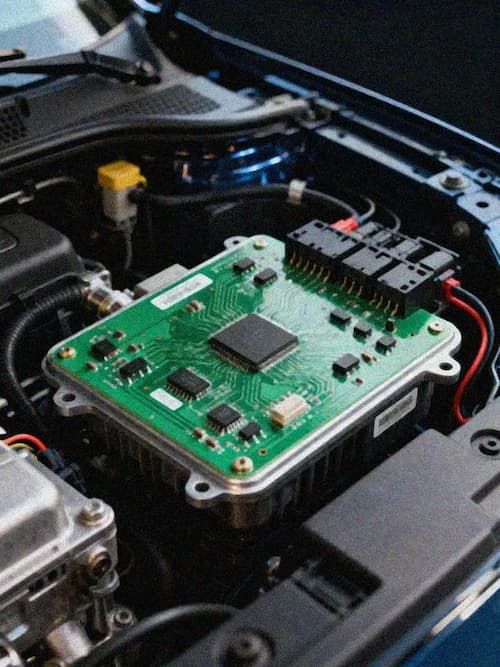
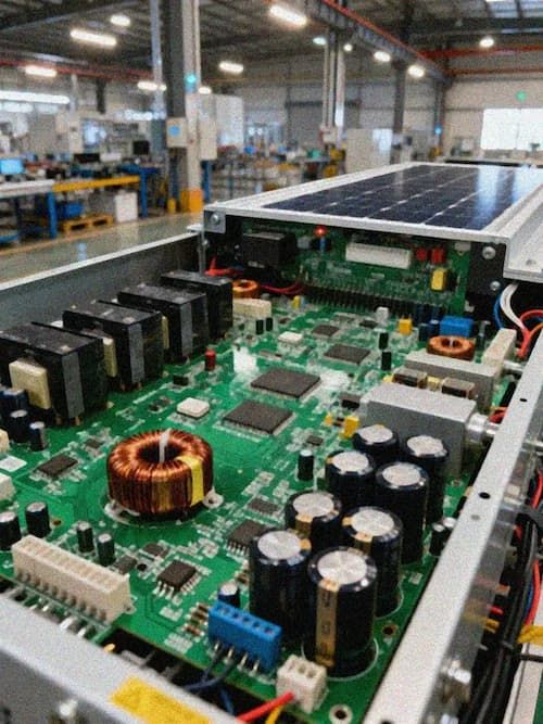
The execution layer PCB directly controls motors, brakes and joint actuators, and is one of the boards with the highest power density inside the robot. A humanoid robot may contain 20 to 50 degrees of freedom, requiring motor drives, current sampling, encoder interfaces, temperature monitoring and protection circuits near each joint. It is not uncommon for peak currents to reach tens of amperes, especially during start-up, braking, sudden load changes, or posture adjustments. The copper foils, power vias and power device pads on the drive board will be subject to transient thermal shocks. If the executive layer PCB design is only estimated based on the average current, it will often underestimate the temperature rise and voltage drop under peak operating conditions.
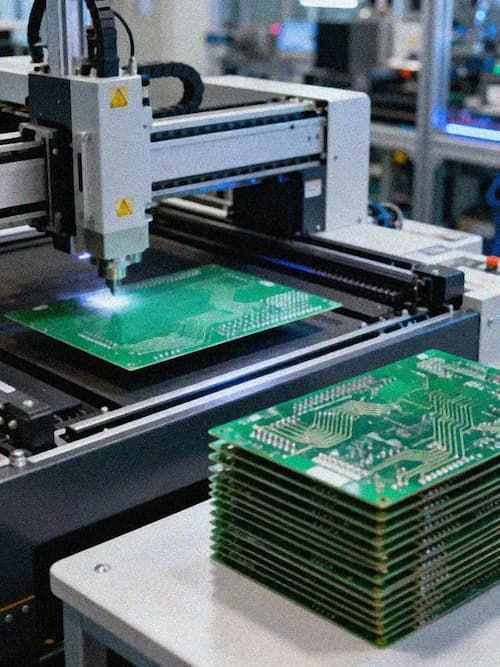
Thick copper plates are a common process choice for execution layers. Increasing the copper thickness from the conventional 1oz to 3oz, 6oz or even higher can reduce on-resistance, reduce I²R loss, and improve short-term overcurrent capabilities. Thick copper is not always thicker, because increasing copper thickness will lead to reduced etching accuracy, increased difficulty in line width compensation, changes in lamination stress, and increased soldering heat capacity. Kingbrother has experience in designing copper plates with thickness of more than 6oz and high current. In projects such as joint drive boards, the manufacturing side needs to evaluate copper thickness, line width, via array, solder resist windows and heat dissipation paths in advance, rather than just based on current tables Give recommendations on copper foil width.
EMC is an engineering problem that cannot be avoided by the PCB of the execution layer. MOSFET or GaN device switches in motor drives produce higher dv/dt and di/dt, and parasitic inductances and discontinuity in the return path can couple noise to the encoder, current sampling, and communication link. The connection position between the power ground and the signal ground, the gate drive loop area, the bus capacitor mounting position, the motor output RC absorption network and connector shielding all determine the passing probability of subsequent EMC tests. Many teams reduce the switching frequency or relax the control parameters to stabilize the system during the prototype stage. After mass production, the parameters are adjusted higher in order to improve efficiency and response speed, and the noise problem in the PCB layout will be re-exposed.
The execution layer should also consider the reliability after thermal cycles and vibration are superimposed. The thermal expansion behavior of thick copper areas and FR-4 substrates is different. Heavy-duty connectors, power inductors and large-package MOSFETs also concentrate stress near solder joints during vibration. For joint drive boards, it is recommended to add thermal cycling, vibration and long-term stalled or high-load operation tests at the template stage to observe whether there are abnormalities in solder joints, vias and copper foil edges. Compared with just looking at the initial functions, the reliability verification before mass production can better reflect the performance of the execution layer PCB in real robot motion.
Inter-board communication: The internal link of the robot needs to be handled according to the system
There are multiple communication links between the robot's internal boards, including EtherCAT, CAN-FD, MIPI, USB, Ethernet and the increasing SerDes channel. EtherCAT is suitable for multi-axis real-time control, CAN-FD is often used for robust control and diagnostic links, MIPI mainly serves cameras and display interfaces, and SerDes is used for scenarios with higher bandwidth, longer distances, or simplified wiring harnesses. The speed and fault tolerance capabilities of different protocols vary greatly, and PCB designs cannot apply fixed rules just based on interface names. For industrial robots PCB design, the communication link also faces long wiring harnesses, aging connectors, vibration and strong electromagnetic interference environments.
High-speed differential links require attention to impedance, loss, return paths and connector transition areas. EtherCAT and high-speed Ethernet usually require a differential impedance of 100Ω. Differential pair length matching needs to be controlled based on rate and protocol budget. MIPI and SerDes also need to focus on insertion loss, return loss, jitter and equalization capabilities. The connector area is a common weak point because the internal trace impedance of the PCB can be controlled through lamination, but the transition between connectors, wiring harnesses and board edges can easily introduce discontinuities. The connectors at the robot joints are also subject to dynamic stresses, and mechanical reliability and signal integrity need to be evaluated together.
The systematic nature of inter-board communication design is also reflected in the processing of power supply and ground. Some problems do not come from the communication protocol itself, but from power supply noise flowing back through the wiring harness, ground potential drift of different cards, and driving board switching noise coupled to the sensing board along the shielding layer. The design stage needs to be clear which links need to be isolated, which links can be shared, and which connectors must be shielded and fixed. For a complete robot, communication reliability cannot be determined only by the eye diagram of a single differential line, but also verified based on the movement of the whole machine, changes in motor load and wiring harness assembly method.
System-level DFM: Risks in mass production are often hidden outside the board
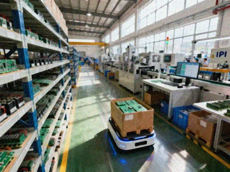
After the single-board design passes the review, the robot control system will also enter into complete assembly, wiring harness layout, EMC pre-scanning, thermal testing and small-batch trial production. The problems exposed at this time often span multiple departments: the structure team changed the heat dissipation path after adjusting the shell, the wiring harness team changed the direction of the connector for ease of assembly, the algorithm team increased the inference frame rate, which led to an increase in power consumption of the main control board, and the control team adjusted The motor parameters increase the noise at the execution layer. If PCB suppliers only participate in manufacturing after Gerber is exported, it will be difficult to help customers identify these cross-system issues. The value of the IPDM (Integrated Product Development and Manufacturing) model lies in connecting design, DFM, proofing, manufacturing and test feedback in series, allowing manufacturing experience to enter the hardware architecture earlier.
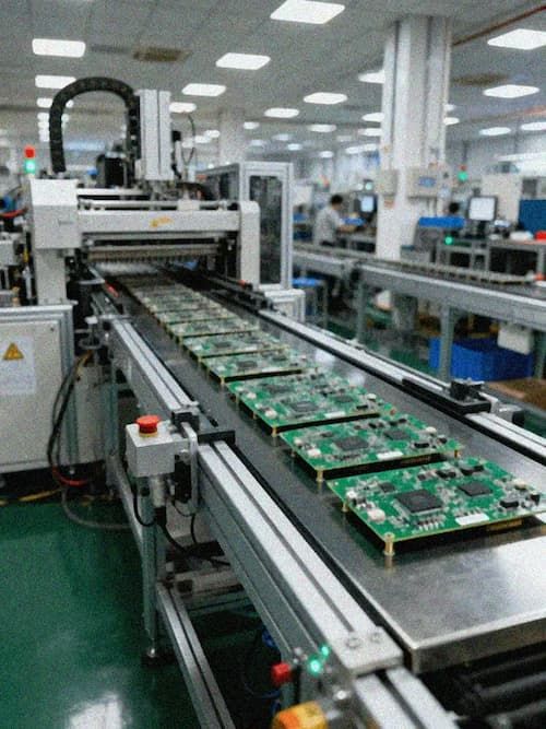
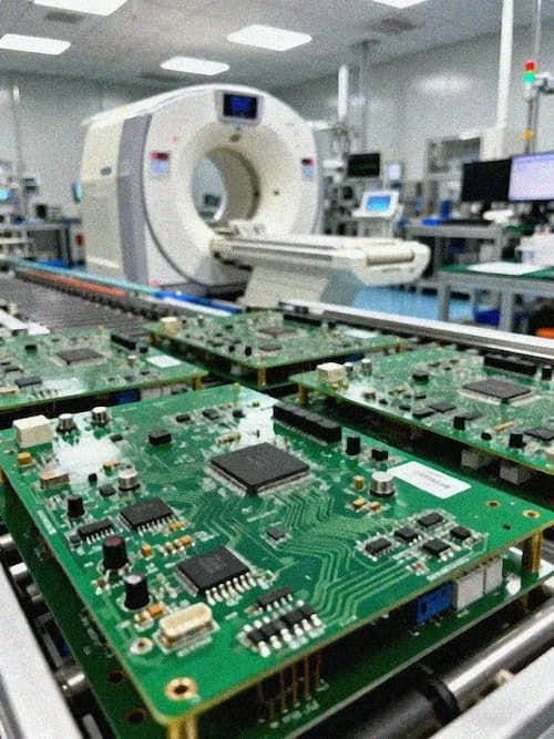
Taking the small-batch import of robot projects as an example, the first round of prototypes usually only verifies functions, the second round of prototypes starts to focus on assembly and stability, and the third round will be close to mass production. If the PCB design ignores connector forces, board edge positioning, radiator installation tolerances and test point accessibility in the first round, each subsequent structural modification may affect lamination, wiring and BOM changes. Kingbrother's IPDM model, robot hardware development experience, and early EMC and DFM evaluation capabilities can help the team detect these risks in advance during the prototype phase. For AI robot companies that need rapid iteration, reducing the number of invalid board changes is often more important than the speed of a single proofing.
In 2026, the robot industry is shifting from displaying prototypes to small batch delivery. The embodied intelligence, humanoid robots and industrial collaborative robots that appear at exhibitions such as CES Asia no longer only display single point functions, but place more emphasis on continuous work, stable grasping, complex scene adaptation and maintenance convenience. This change will push PCB requirements towards long-term consistent operation, rather than being satisfied with functional lighting during the prototype stage. Suppliers with HDI high-level numbers, rigid-flexible combination, thick copper power boards and system-level DFM support will more easily adapt to the complex needs of AI robot control systems. For the hardware team, when selecting a PCB solution, board performance, manufacturing window, reliability verification and complete machine assembly should be placed in the same decision table, rather than supplementing the mass production design after the prototype is successful.