Apple introduced its next-generation Apple Intelligence platform and Siri AI assistant at WWDC 2026 on June 9. With a standalone Siri app and deeper system-level AI features in iOS 27, on-device AI has moved from a software promise into an actual hardware requirement. Around the same time, Gartner projected that global AI PC shipments would reach 143 million units in 2026, with penetration exceeding 50% for the first time.
The broader implication for electronics manufacturing is clear: AI is no longer limited to data centers. More inference workloads are moving into phones, PCs, tablets, wearables, and industrial edge devices. Stronger NPUs, larger local memory, higher power density, and more demanding thermal designs will all flow downstream into PCB design and fabrication.
The Shift from Cloud AI to Device AI
Over the past two years, most consumer AI workloads have been processed in the cloud. A user sends data to a large model running in a data center and receives the result back over the network. On-device AI changes that architecture by running inference locally, reducing network dependency and improving response time for privacy-sensitive or latency-sensitive functions.
The tradeoff is hardware intensity. Running a compact language model locally typically requires 8GB to 16GB of DRAM for model loading, prompt handling, and inference buffering, while higher-end use cases are already pushing toward 32GB configurations. This comes at an awkward time for device makers because memory pricing has been rising sharply through 2026. The device industry is therefore being asked to add memory capacity just as memory costs are becoming harder to absorb.
The processor side is just as demanding. A more capable NPU generally brings higher transistor density, more localized heat, and more complex power delivery behavior. Future mobile SoCs are expected to dedicate more silicon area to neural processing, and that will place additional pressure on package substrates, main logic boards, and board-level interconnect. Finer line widths, tighter spacing, more signal layers, and more complicated stack-ups will become increasingly common in high-end devices.
Where Smartphone PCB Design Gets Harder
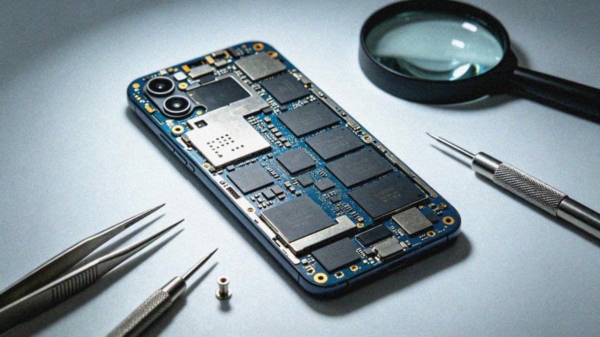
Power density is the most immediate constraint. During local AI inference, a mobile SoC can produce short bursts of power draw far above a typical application workload. Those bursts create localized hot spots around the processor, PMIC, and memory region, which means thermal paths need to be considered at the PCB layout stage rather than treated as a late mechanical design issue. Copper thickness, thermal via density, ground plane continuity, and the placement of heat-spreading structures all become part of the same design problem.
Signal integrity is becoming more difficult as well. Data movement between the NPU, DRAM, storage, camera modules, and wireless subsystems increases as AI features become more interactive. Faster memory interfaces demand tighter length matching, more careful impedance control, and stronger crosstalk management. In a smartphone main board, there is little spare area to solve these problems by simply spreading traces out, so the burden shifts toward HDI manufacturing accuracy and stack-up discipline.
The stack-up itself is also changing. To fit more interconnect channels into a limited board area, high-end phones are expanding their use of any-layer HDI and SLP (Substrate-like PCB) construction. Some flagship main boards have moved from roughly 10 layers toward 12 to 14 layers, depending on model architecture and RF layout. Once layer counts increase and via structures become denser, registration drift, microvia fatigue, and resin flow variation become more difficult to control during volume production.
AI PCs and AI Phones Share the Same Engineering Direction
Gartner's AI PC forecast points to the same hardware direction now appearing in smartphones. Qualcomm's Computex 2026 message that agents will make devices more central to computing reflects a wider shift in system design: more intelligence is being placed close to the user, not only in cloud infrastructure. PCs have more room for heat spreaders, larger batteries, active cooling, and wider board areas; smartphones must solve similar problems in a much tighter mechanical envelope.
For PCB suppliers, this changes the meaning of consumer electronics capability. Standard HDI capacity is no longer enough for premium device programs. Customers are increasingly looking for finer trace geometry, more reliable stacked microvias, stable dielectric behavior at higher interface speeds, and stronger process control across large production lots. Moving from 40μm/40μm lines and spaces toward 30μm/30μm or below requires more than updated design rules; it requires tighter imaging, cleaner etching, better copper plating control, and stronger inspection coverage.
Materials are also moving up the performance curve. High-speed NPU-to-memory data paths are more sensitive to dielectric constant (Dk) and dissipation factor (Df) variation than traditional mobile application boards. Conventional FR-4 remains useful in many sections of a handset board, but modified epoxy systems and medium-loss materials are becoming more attractive where insertion loss and signal margin need to be controlled. The difficulty is that these materials can narrow the lamination process window, especially when thin cores, stacked microvias, and dense BGA escape routing are combined in the same design.
What Supplier Qualification Will Need to Measure
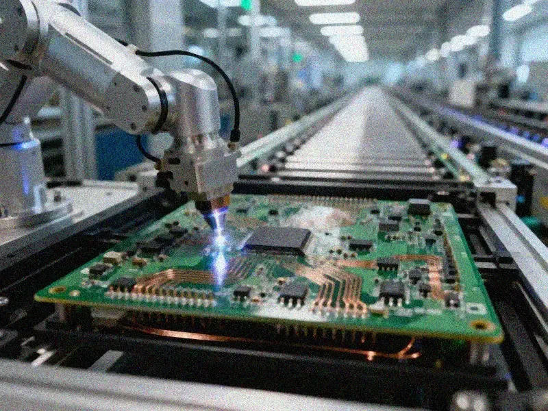
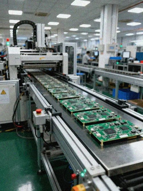
A major Asia-Pacific PCB manufacturer brought its third-generation any-layer HDI line into production in early 2026 for smartphone and wearable device programs. The line was designed for AI-capable main boards, with four-layer stacked via structures and minimum line/space capability around 28μm. From equipment installation to customer qualification, the program took roughly 10 months, with microvia reliability testing alone consuming nearly three months. The main yield issue during early pilot builds was not open circuits; it was intermittent resistance shift after thermal cycling, caused by small variations in copper plating thickness inside stacked via structures.
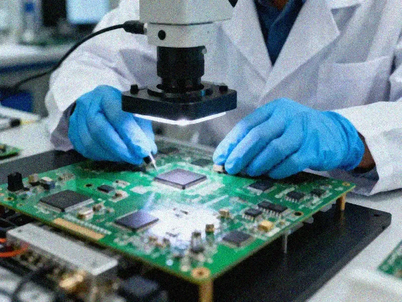
This kind of qualification work is becoming more common. On-device AI does not change every smartphone PCB overnight, but it raises the technical ceiling for premium products. Once a device program combines higher NPU power density, larger memory packages, high-speed interfaces, and a thinner mechanical profile, the board supplier must support HDI fabrication, thermal design review, material selection, and reliability validation as an integrated engineering task.
For procurement teams, the supplier evaluation checklist should therefore look beyond price and nominal capacity. Useful questions include whether the supplier is investing in next-generation HDI lines, whether it can support thermal and signal-integrity reviews before layout release, whether it has process data for stacked microvia reliability, and whether it can maintain line-width, plating, and registration control across high-volume production. In the on-device AI cycle, the strongest PCB suppliers will be those that can turn advanced design rules into stable manufacturing outcomes.