SEO Description: The power consumption of AI accelerators is moving from hundreds of watts to kilowatts, and the high thermal conductivity pcb has become a key link in the thermal management chain. This paper analyzes the engineering boundaries of AI accelerator PCB thermal management from the perspectives of material system, thermal vias, embedded copper blocks, liquid-cooled contact surfaces and material selection.
Body
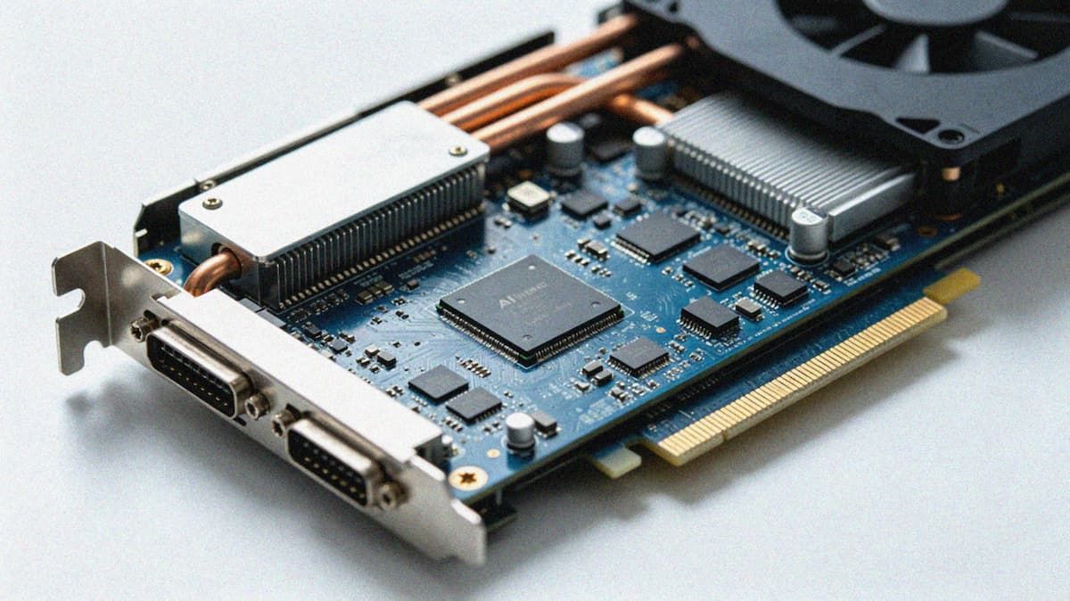
The power consumption of AI accelerators has entered a range that is difficult to handle with traditional server experience. The typical power consumption of the NVIDIA A100 is between 250W and 400W. The H100 platform has pushed the power consumption of a single card to the 700W level. After CompuTEX 2026, discussions around the Vera Rubin platform have pushed the power consumption of the next generation GPU to more than 1000W. The increase in power consumption itself is not new. What changes the boundaries of PCB design is the concentration of heat in smaller chip packages, higher-bandwidth HBM stacks and denser power supply areas. For AI servers and accelerator cards, heat dissipation is no longer borne by the heat sink or cold plate alone, and the role of PCBs in the heat conduction path is significantly increasing.
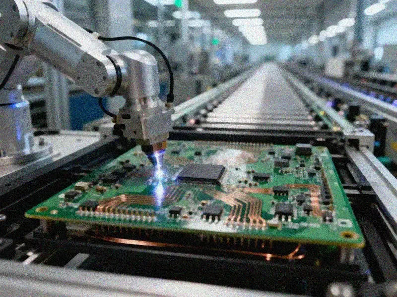
The heat generated by the chip needs to pass through Thermal Interface Material (TIM), package substrate, PCB copper layer, thermal via, metal substrate or embedded heat dissipation structure, and finally conducted to the cold plate, air duct or liquid cooling system. The thermal conductivity of traditional FR-4 materials is usually only 0.3 to 0.4 W/m·K, and the thermal conductivity of copper is about 385 W/m·K, a difference of nearly three orders of magnitude. At this power consumption level, each thermal resistance inside the PCB will be amplified, and local hot spots may cause chip frequency reduction, power device life shortened, solder joint fatigue and material stratification. The value of high thermal conductivity pcb lies in extending thermal management from external heat sinks to the interior of board-level structures, allowing materials, copper thickness, thermal channels and mechanical contact surfaces to jointly assume the task of thermal diffusion.
High thermal conductivity PCB material system: FR-4, boundary between metal substrate and ceramic substrate
Most AI accelerator motherboards are still based on high-TG FR-4. TG170 + grade plates have better size stability and mechanical strength in high temperature environments, and are suitable for carrying high-layered layers, high-speed signals and more complex power supply planes. Its limitations are also clear: the thermal conductivity will not be significantly improved by the increase in TG value, and the thermal diffusion on the board still relies mainly on copper foil, thermal vias and local heat dissipation structures. For device areas of the 100W to 300W level, high TG FR-4 can usually still work with thick copper layers and thermal via arrays; as power consumption continues to rise, the conventional FR-4 structure alone will make the margin for thermal simulation very narrow.
Metal Core PCB (MCPCB) is more suitable for medium and high power consumption devices. Aluminum substrates are very mature in LEDs, power modules and some power electronic products. The equivalent thermal conductivity after containing an insulating dielectric layer is generally 1 to 3 W/m·K; copper substrates are more costly and heavier, but can provide better thermal and current carrying capabilities, and some structures can reach 5 to 10 W/m·K or even higher. The core path of the metal substrate is to allow the device heat to pass through the insulating layer and quickly enter the metal core, and then be conducted by the metal core to the cold plate or enclosure. The thickness of the insulation layer, the thermal conductivity of the medium, the flatness of the metal core and the pressing force of the cold plate will all affect the final thermal resistance.
Ceramic substrates are often used in more extreme thermal management scenarios. The thermal conductivity of aluminum oxide (Al ˇ O) ceramic substrates is about 20 to 30 W/m·K, and aluminum nitride (AlN) can reach 170 to 200 W/m·K, and the thermal expansion coefficient is closer to that of silicon chips. It has a good reliability foundation under thermal cycling conditions. Its engineering costs are also obvious: processing is difficult, size is limited, cost is high, and complex multi-layer interconnection capabilities are not as flexible as traditional PCB systems. Therefore, in AI accelerator systems, ceramics appear more in power modules, radio frequency devices or local high heat flow density areas, and the direct replacement of entire server motherboards is still limited.
| material type | Typical thermal conductivity | processing difficulty | cost level | applicable scenarios |
|---|
| Ordinary FR-4/High TG FR-4 | 0.3-0.4 W/m·K | low | low to medium | High-level motherboards, universal accelerator cards, hot vias and thick copper required |
| aluminum substrate | 1-3 W/m·K | in | in | Medium and high power consumption power supply areas, LEDs and some power modules |
| copper substrate | 5-10 W/m·K | middle and high | middle and high | High power density devices, local heat dissipation enhanced structures |
| Alumina Ceramic | 20-30 W/m·K | high | high | Power modules, local heat sources with high reliability requirements |
| aluminum nitride ceramic | 170-200 W/m·K | high | very high | Applications with extremely high heat flux densities and stringent CTE matching requirements |
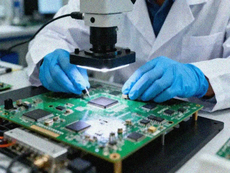
Kingbrother's accumulation in TG170 + high-TG plates, metal substrates, ultra-thick copper and thermoelectric separation processes is suitable for early plan review of AI accelerator thermal management PCBs. Material selection cannot only look at the thermal conductivity table, but also look at the target number of layers, impedance control, drilling ability, copper thickness compensation, lamination stability and mass production yield. A material that performs well in thermal conductivity will also be limited in its help to AI hardware projects if it cannot carry high-speed differential lines, dense BGA fan-out, or stable mass production.
Hot vias, thick copper and embedded copper blocks determine the internal heat channels on the board
Thermal vias are the most common board-level heat dissipation method in FR-4 systems. Designers will place dense copper-plated holes under the GPU, VRM, power MOSFET, or high-power chip to allow heat to pass vertically through the dielectric layer into the underlying copper surface or cold plate area. Common aperture sizes are between 0.2 and 0.3 mm, and spacings can be arranged in a grid of 0.5 to 1.0 mm, depending on pad size, insulation spacing, manufacturability and risk of solder voids. There is still air thermal resistance inside unfilled thermal vias. Copper filling or conductive filling can significantly improve thermal conductivity, but it will also increase processing complexity and cost.
Hot via design is easy to underestimate because it affects heat dissipation, soldering, and signal integrity at the same time. If the number of vias is too small, the heat under the chip is difficult to be discharged in time; if the number of vias is too large, solder paste loss, voids increase or mechanical stress concentration may occur in the pad area. For high-speed accelerator cards, hot vias may also compress the BGA escape space, interrupt the continuity of the reference plane, and affect the reflow path of high-speed differential lines. Kingbrother's 0.2mm laser drilling and high-density hole processing capabilities can provide a manufacturing basis for such hot via arrays; hole arrays still need to be evaluated together with bond pad design, solder resist windows and laminated structures.
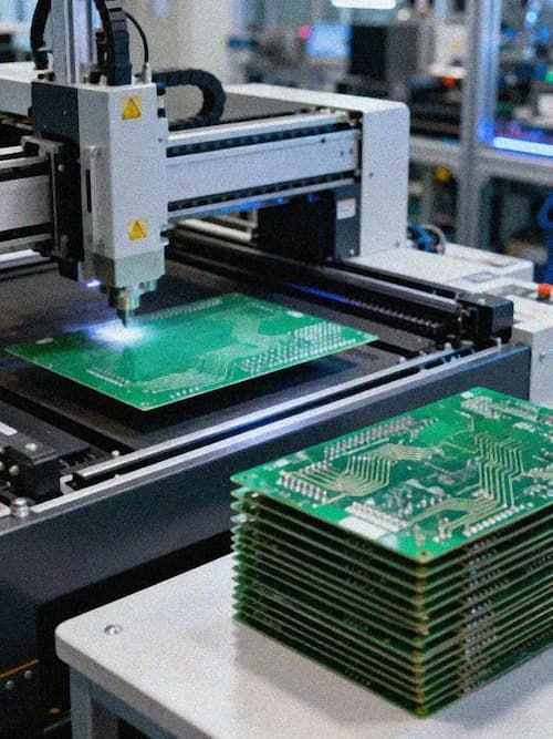
Thick copper layers are suitable for areas that need to handle both high currents and heat dissipation. The current density of the AI accelerator power supply module is very high, and the periphery of the VRM often requires a copper thickness of 2oz, 3oz or even higher to reduce conduction losses and temperature rise. The ultra-thick copper process can improve current carrying capacity, but it also brings problems such as etching compensation, lamination filling, line width control and local copper density balance. When the thick copper area and the thin wire high-speed signal area are placed on the same board, the manufacturing window will narrow, and the lamination and zoning design must be planned in advance, otherwise it will be difficult to meet the power supply integrity, impedance control and board warping requirements at the same time in the later stage.
For localized areas with higher heat flow densities, embedded copper blocks or copper Coin can provide shorter heat paths. The copper block is usually embedded inside the PCB, and the heat from the chip or power device is directly transferred into the high thermal conductivity copper structure through the solder pads, and then conducted to the cold plate contact surface on the back. Copper Coin may be as thick as 2 to 5mm, and its thermal conductivity is close to pure copper; it is not completely consistent with the thermal expansion behavior of FR-4 substrate. During thermal cycling, stress concentrations may occur at the edges of copper blocks, resin-filled areas and adjacent copper layers, which may lead to delamination, micro-cracks, or solder joint fatigue. Therefore, embedded copper blocks cannot be simply understood as putting copper into the board. This is a process that requires joint verification of material, lamination, mechanical and reliability testing.
Air cooling, liquid cooling and hybrid cooling in AI hardware thermal design
Air cooling still exists in low and medium power AI accelerators and some edge AI hardware. Its advantages are mature systems, simple maintenance, relatively controllable costs, and low requirements for PCB surface treatment and liquid leakage protection. For devices of the 300W to 500W level, the air-cooling system can still meet the requirements under certain conditions with hot vias, thick copper, local copper surface diffusion and reasonable device layout. Limiting air duct space, noise, radiator size and chassis wind resistance, as power consumption continues to rise, air cooling requires a very large cooling structure to maintain acceptable junction temperatures.
AI accelerators above 700W are pushing liquid cooling into the mainstream. Cold plate liquid cooling directly adheres to the surface of the chip or module through the thermally conductive interface material. The cooling liquid carries away heat in the cold plate channel, and the thermal resistance is significantly lower than that of traditional air cooling. Liquid cooling systems have put forward new mechanical and material requirements for PCBs: cold plate mounting hole location, pressing force distribution, board flatness, local bare copper or nickel plated palladium treatment, leak-proof area isolation and sensitive device avoidance, all need to be determined during the layout stage. If the cold plate is pressed unevenly, local differences in the thickness of the TIM will occur, eventually causing hot spots to migrate or temperature fluctuations.
Hybrid cooling solutions are becoming increasingly common in high-end AI servers. Front cold plate liquid cooling can handle the main heat source near the GPU and HBM, back vapor chamber (VC) or heat pipe can diffuse local hot spots on the back of the PCB, and on-board hot vias and copper layers undertake vertical and planar heat conduction. TIM materials also affect system performance: thermally conductive silicone grease is usually 1 to 5 W/m·K, thermally conductive gaskets are about 3 to 8 W/m·K, and liquid metals can reach 20 to 80 W/m·K, but it places additional requirements on surface treatment, material compatibility and long-term reliability. In engineering practice, the materials with the highest thermal conductivity may not be the most suitable for mass production, because coating consistency, pumping effects, corrosion risks and ease of maintenance can also affect system life.
A common debugging scenario is that the accelerator card passes the temperature in the open environment of the laboratory, but the frequency is partially reduced after being installed in a high-density cabinet. Preliminary inspection showed that the water temperature in and out of the cold plate was normal, and the problem was finally located in the VRM area on the back of the PCB and local hot spots near the connector. The root cause of the problem lies not in the cold plate capacity, but the hot channels on the board do not effectively channel back heat into the main cooling path. The local copper area is limited by high-speed signal wiring and mounting holes, and the amount of TIM compression also varies. Subsequent versions stabilized by adjusting the copper plane, adding thermal vias, improving the cold plate crimping area, and redistributing high-power device locations. Such problems indicate that AI hardware thermal design needs to put chips, PCBs, cold plates, chassis and fluid systems in the same thermal model for collaborative evaluation.
Selection of high thermal conductivity pcb depends on constraints other than thermal conductivity
Material selection usually starts with power consumption and heat flow density. In device areas ranging from 100W to 300W, priority can be given to evaluating the combination of high TG FR-4, thick copper and hot vias; between 200W and 500W, the value of metal substrate or local copper block solutions will increase; higher heat flow densities or areas with strict requirements for CTE matching, ceramic substrates and special composite materials are more worthy of entering the candidate list. This division can only be used as a preliminary judgment, as package size, cold plate contact conditions, ambient temperature, workload and reliability criteria all change the thermal design margin.
CTE matching is another factor that can easily be ignored early on. Highly thermally conductive materials tend to be harder and more fragile, or have different expansion behaviors with FR-4, copper, and silicon chips. AI accelerators undergo thermal cycling after long periods of high-load operation, and stresses between chip packaging, solder joints, PCB media and cold plates continue to change. The higher the thermal conductivity of the material, if the mechanical matching is not well handled, the problem may be transferred to solder joint fatigue, delamination or microcracks. Reliability testing needs to cover thermal cycling, thermal shock, damp heat, bending and long-term power aging, rather than just looking at the peak temperature of a single thermal simulation.
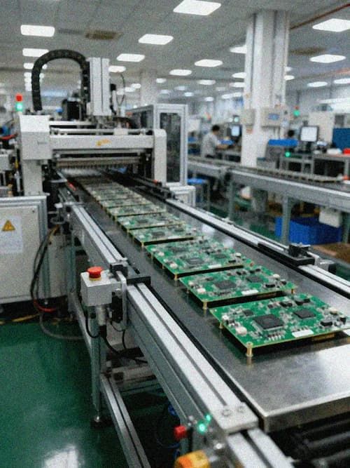
Cost and processability determine whether a solution can enter mass production. Ceramic substrates and embedded copper blocks can solve local thermal problems, but may bring longer delivery times, lower yields and more complex assembly processes; metal substrates have advantages in heat dissipation, but multi-layer high-speed signals, BGA fan-out and fine-pitch device layout will be limited; high TG FR-4 costs and processing maturity are the best, and thermal performance needs to rely on structural compensation. For procurement and hardware teams, when selecting a metal core PCB manufacturer, in addition to confirming aluminum or copper substrate manufacturing capabilities, they also assess whether they understand high-speed signals, power supply networks, cold plate assembly and reliability verification in AI accelerators.
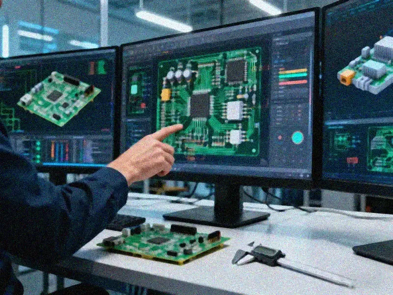
PCB manufacturers such as Kingbrother with high-TG plates, metal substrates, ultra-thick copper, embedded copper blocks and thermoelectric separation capabilities are more suitable to participate in early DFM and thermal design reviews. The sooner suppliers see chip power consumption, package size, cold plate structure, BGA fan-out, device height limitations, and target test conditions, the easier it will be to determine whether materials and process solutions can be mass produced. For high-end AI hardware projects, reducing one hot design rework is often more valuable than simply compressing the proofing cycle.
GPU power consumption continues to rise, PCB thermal management will be closer to the center of system design
The signal from the Vera Rubin platform is clear: AI accelerators are evolving towards higher power consumption, higher memory bandwidth, and higher integration density. After GPU power consumption enters the 1000W level, PCB thermal management will shift from auxiliary design to part of the system architecture. FR-4 heated vias will still exist, but they are more likely to assume the role of basic interconnection and local thermal diffusion; metal substrates, copper Coin, temperature equalizing plates, liquid-cooled contacts and new highly thermally conductive insulating materials will be used in high-power areas Get more application space.
In the next five years, the development of high thermal conductivity PCB will advance in several directions. New highly thermally conductive composite materials may improve thermal conductivity while maintaining processability. 3D packaging and Chiplet architecture will change the way heat sources are distributed. AI-assisted thermal simulation will help engineering teams identify hot spots and thermal stress risks early in design. At the same time, process stability at the manufacturing end will become more important, because after high thermal conductivity materials, thick copper, embedded structures and high-layer stacks are combined, fluctuations in any link may affect the yield. PCB suppliers that can combine material selection, board-level heat dissipation, cold plate assembly, and mass production of DFM will be closer to the core of AI accelerator hardware development.