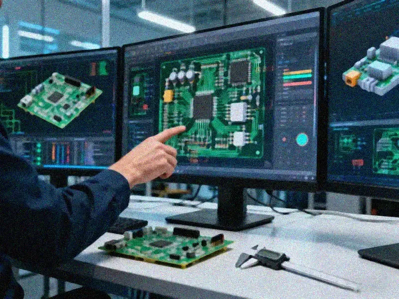
Edge AI has moved inference workloads out of the data center and onto the device, but that shift has not made hardware design any easier. An edge inference board has to satisfy four constraints at once: compute, power, physical size, and thermal budget. The factor that ultimately decides whether it can ship at volume is usually not the chip itself but the PCB engineering around it. For a team planning an edge AI product, thinking about selection, stack-up, power, thermal, and manufacturing as one chain is more valuable than picking an NPU in isolation.
NPU Selection and System Architecture
The starting point for edge AI hardware is balancing inference capability against a power budget. The RK3588's 6 TOPS NPU targets lightweight vision and voice workloads, while the Jetson Orin family spans tens to hundreds of TOPS and discrete accelerators such as the Hailo-8 offer a more specialized path. Selection depends on whether the chip can run real-time inference on-device, which requires weighing model quantization precision, memory bandwidth, and interface needs together; raw TOPS alone is a poor guide.
NVIDIA put that shift into sharp focus at the end of 2024 when it priced the Jetson Orin Nano Super developer kit at $249 with 67 TOPS of INT8 performance, positioning it as a generative AI platform for small edge devices. That price point lowered the cost of entry for edge AI hardware and gave more teams a way to validate an inference design on-device before committing to volume production.
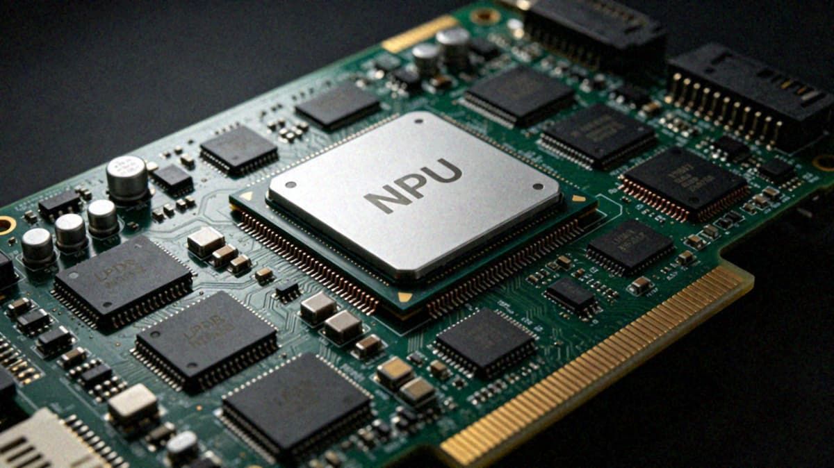
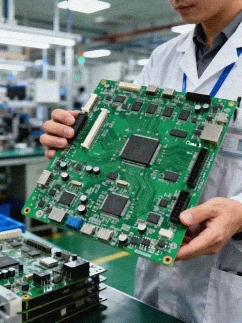
SoC-integrated NPUs and discrete NPU modules are two different architectural routes. The integrated approach saves board area and reduces system complexity, which suits consumer and compact devices; a discrete module provides more compute headroom and thermal margin, which suits sustained, high-load industrial and robotics use cases. Either way, the memory subsystem is the part that gets underestimated. LPDDR4X/5 signaling places strict demands on trace length, length matching, and power integrity, and the stack-up and routing approach directly determine how stable inference latency remains.
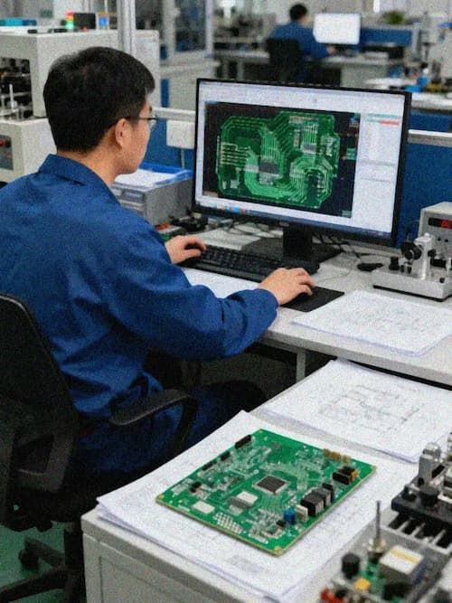
Edge inference boards typically land in the 8-12 layer range. Layer count has to serve power integrity, high-speed return paths, and signal isolation at the same time, and adding layers alone does not fix signal problems; the key is a sensible allocation of ground and power planes. High-speed differential pairs target 100 ohms, while USB, PCIe, and MIPI interfaces each carry their own length-matching and return-path requirements. Any discontinuity in the return path turns into crosstalk and jitter.
KINGBROTHER has already exercised a 10-layer, 100-ohm, 750 Gbps I/O design on a Jetson Xavier evaluation board, and that reference design validated the feasibility of carrying high-speed I/O and power networks together within a limited layer count. For most edge projects, that kind of working reference is more useful than building a stack-up from scratch.
Thermal and Power Management
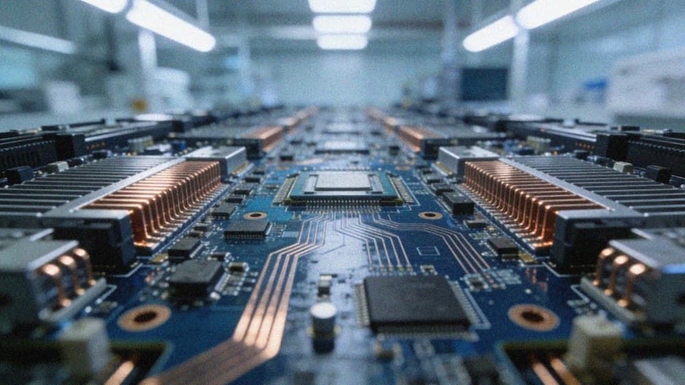
Edge devices have limited space, so thermal design usually has to be handled at the board level. Thermal vias carry heat from the chip pad to the copper pour and the heatsink surface, while thermal pads and thickened copper reduce hot-spot temperature. Power tree design is just as important: with multiple low-voltage rails and dynamic loads, the placement and ESR/ESL characteristics of decoupling capacitors directly affect voltage ripple and transient droop.
Manufacturing and HDI
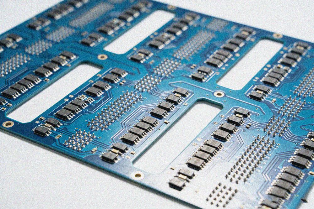
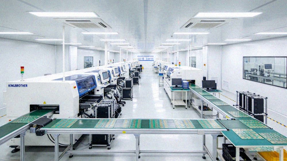
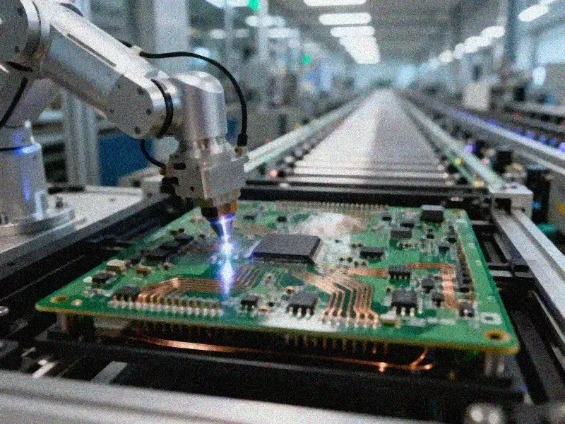
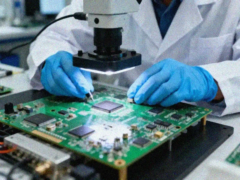
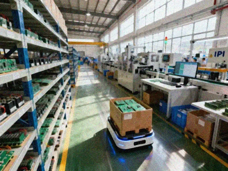
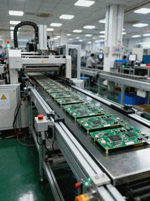
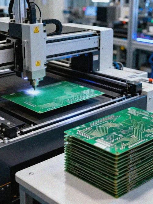
The manufacturing challenge for inference boards concentrates in HDI and high-frequency materials. Dense routing needs fine line width and spacing plus microvia processes, while high-frequency materials determine signal loss over long paths. KINGBROTHER's capabilities span 72-layer FR4 samples and 32-layer volume production, 30-layer any-layer HDI samples and 26-layer four-step HDI in volume, high-speed materials including TU933+/TU943N and Panasonic M6-M8N, and impedance control to ±5%/±10%. Those parameters let a board move smoothly from prototype to volume without discovering a manufacturing incompatibility only after the design is frozen.
Closing
The competitiveness of edge AI inference hardware ultimately comes down to a clean handoff between design and manufacturing. NPU selection, stack-up planning, power and thermal design, and HDI manufacturing all have to align, because a disconnect in any one of them delays time to market. Teams that are still weighing stack-up and power options can bring those parameters to an engineering review, where the conclusion tends to be closer to what can actually be produced.