The Shenzhen International Convention and Exhibition Center (Bao 'an)* High-tech Achievements Fair held in November every year is a noteworthy observation window for the global electronics industry. CHTF has spanned more than 20 years since its establishment. It has gradually evolved from an early comprehensive exhibition focusing on display of results to an industrial docking platform covering more than 20 cutting-edge fields such as artificial intelligence, semiconductors, energy storage, intelligent manufacturing, and low-altitude economy. From November 26 to 28, 2026, the 28th CHTF will once again kick off in Bao 'an, with an exhibition area of 400,000 square meters, more than 5000 brand exhibitors, more than 450,000 professional visitors expected, and more than 120 countries and regions. Participation makes it one of the largest technology exhibitions in the Asia-Pacific region. For global practitioners in the PCB industry, the reference value of CHTF lies in providing a panoramic technical scanning opportunity: in the same exhibition hall, AI computing hardware, embodied intelligent robots, energy storage systems and semiconductor packaging The four major areas are concentrated on the appearance, and these four directions happen to be the current market segments with the most intensive PCB demand and the highest technical specifications requirements.
AI Computing Server Motherboard: Rigidity Requirements for High-Layer and High-Speed Materials
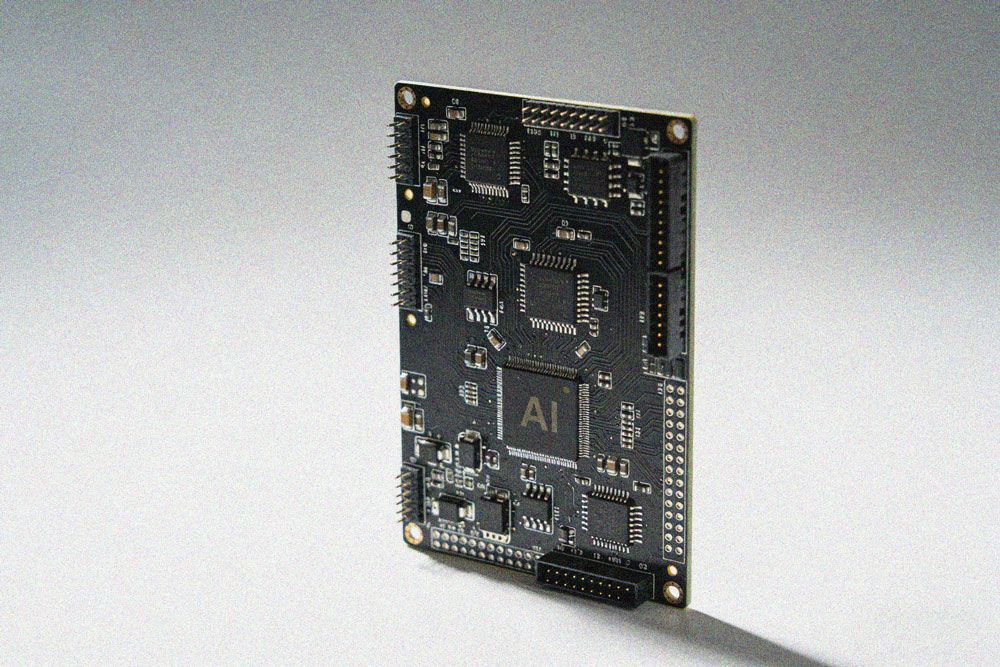
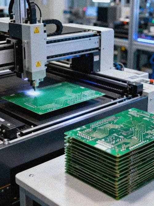
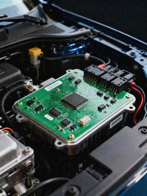
The continuous expansion of AI training and reasoning computing power is profoundly changing the technical specifications of server motherboards. From the GPU substrate to the OAM connector carrier board, to the system-level backplane, the signal rate of the AI server has experienced a leap from 56Gbps PAM4 to 112Gbps PAM4 in the past three years. The engineering verification of 224Gbps has been carried out in some leading manufacturers 'laboratories. The increase in signal rate has directly pushed up the requirements for PCB material systems, and high-speed CCL (copper clad laminate) materials with low loss, low dielectric constant, and low dielectric constant temperature drift have become standard. Taking the current mainstream AI computing server motherboards as an example, the typical specifications have climbed to 16 to 32 layers. It uses ultra-low loss plates of TU933 + grade. The minimum aperture is compressed to 0.2mm, and the line width and line spacing reaches 4.5/2.5mil. It is generally necessary to control the residual pile effect. These parameters were almost sample-level capabilities five years ago, but now they have entered the stage of large-scale mass production.
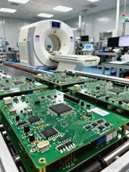
The richness of the material system is becoming a core capability indicator for AI hardware PCB suppliers. In KINGBROTHER's PCB Capabilities 2026 technical matrix, the high-speed material system has covered mainstream brands such as TU933 +, TU943N, Panasonic M6/M7N/M8N, and Shengyi HSD7/HSD8. The FR4 model capacity has reached 72 layers and 32 layers of mass production. Such material coverage and depth of layers allow the same supplier to flexibly match material plans based on customers 'loss budgets, cost constraints and delivery requirements, rather than passively waiting for a certain material's supply window. Judging from the exhibitor structure of CHTF in previous years, the AI computing hardware exhibition area is usually the home of server manufacturers, GPU manufacturers and high-speed connector manufacturers. The participation of PCB manufacturers has increased significantly in the past two years. This change itself shows that the role of PCB in the AI computing power supply chain is changing from passive support to active collaboration, and the weight of high-speed interconnection design capabilities and material engineering experience in customer selection continues to increase.
Shaped intelligent robot: Composite requirements for PCB capabilities in multi-board systems
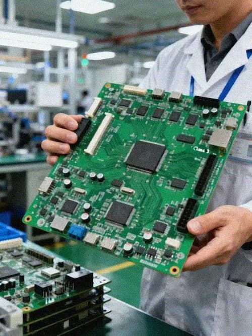
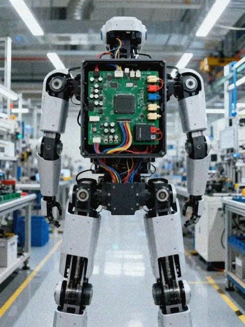
The robot exhibition area of CHTF 2026 is expected to be the stage for the concentrated appearance of humanoid robots and industrial collaborative robots, and the implementation of the concept of embodied AI is pushing the internal electronic architecture of these robots to unprecedented complexity. A typical humanoid robot contains more than ten PCBs, including a head control board, a chest main control board, multiple joint drive boards, a communication board, a power management board, and a sensor acquisition board. Each board undertakes different functions, and the technical requirements are also completely different: The main control board needs to handle high-speed data streams and multiple power domain power supply. The communication board requires the integration of multiple communication protocols such as Wi-Fi, Ethernet, CAN and RS485 in a limited space and meets strict EMC standards. The joint driver board faces the triple pressure of high current, high power density and extreme heat dissipation conditions.
High-speed signal processing capabilities become equally critical in the robot's main control system. With the increased requirements of embodied intelligence for real-time sensing and multimodal data processing, the high-speed signal rate inside the robot has approached the level of 112Gbps, which is in the same order of magnitude as the AI server motherboard. KINGBROTHER's humanoid robot IPDM solution relies on a 56-layer/112Gbps high-speed PCB design capability to cover the high-speed signal requirements of the robot's main control system. The modular design reuse rate reaches 68%, far exceeding the industry average of 35%. It can effectively reduce R & D cycles and mass production costs. In terms of EMC, the first pass rate of 98.5% ensures the stable operation of the robot in complex electromagnetic environments. This solution is developed based on S1000H substrate and has served many humanoid robot enterprise customers.
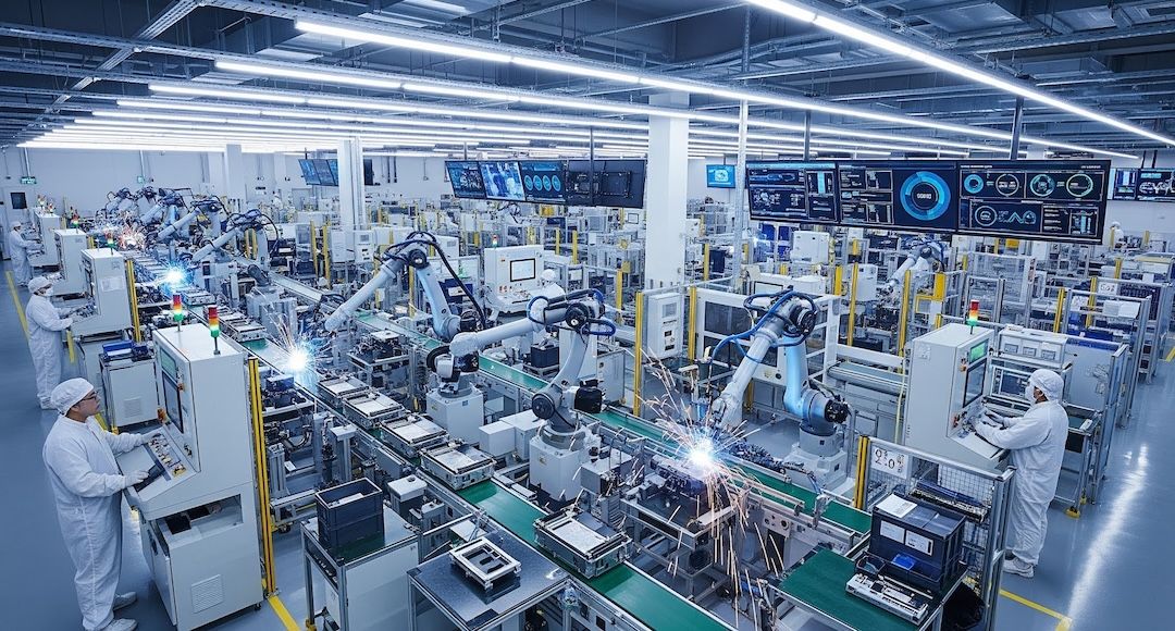
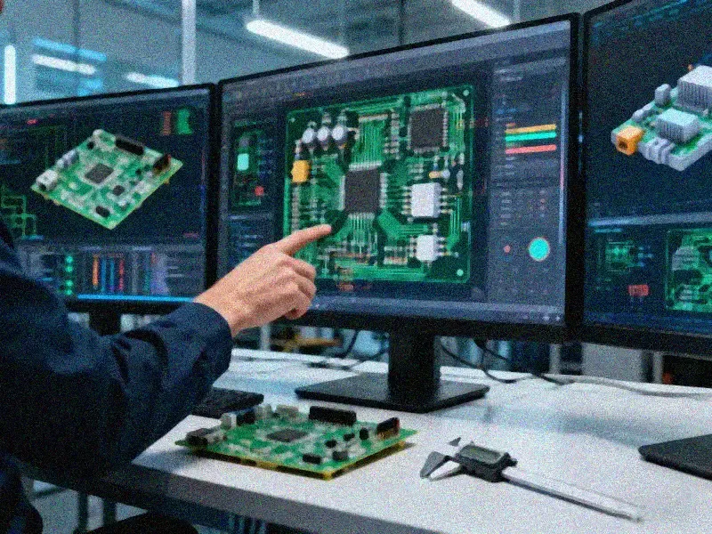
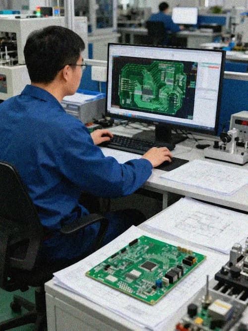
An actual engineering case can illustrate the manufacturing complexity of this multi-board system. In a recently delivered humanoid robot core control board project, the main control board is equipped with a high-performance processor. Three independent power domains need to be designed to supply power to the processor core, communication interface and sensor array respectively, while meeting vehicle specification design standards and composite cooling requirements. The matching joint drive board uses thick copper technology to withstand high current loads, and accurately arranges current sampling resistors and temperature sensors in a limited space. The contradiction between Layout density and heat dissipation path design runs through the entire engineering iteration process. In the end, design, PCB manufacturing and PCBA assembly were integrated into a single service chain through the IPDM model, and the project's cycle from first edition proofing to mass production delivery was reduced to about 60% of the industry average. Judging from the forward-looking information of CHTF 2026, it is expected that dozens of new robots will be released for mass production plans. These orders will form a substantial test for PCB suppliers 'batch consistency and supply chain response speed.
Energy storage system PCB: The reliability competition from BMS to power conversion
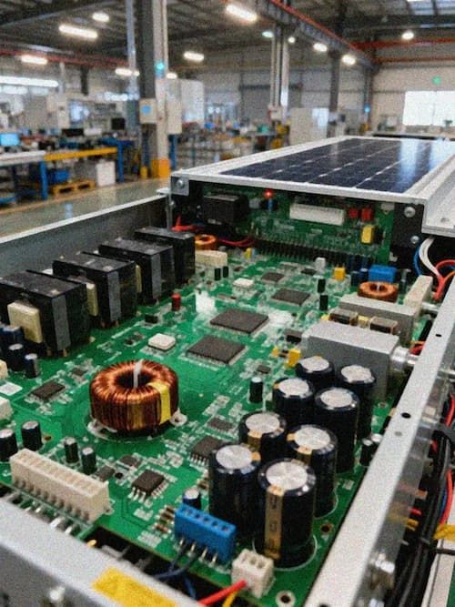
The installed capacity of the global energy storage market has maintained rapid growth between 2025 and 2026. The energy storage and battery exhibition area of CHTF 2026 will be a centralized display platform for this trend. The PCB requirements of energy storage systems are distributed among the three core subsystems: BMS (Battery Management System), PCS (Power Conversion System) and EMS (Energy Management System). Each subsystem has different technical focuses on PCB. BMS focuses on voltage sampling accuracy, long-term reliability and anti-interference capabilities. The voltage and temperature data of hundreds of battery cells often need to be accurately collected through the sampling circuit on the PCB. Any sampling error may lead to overcharging of the battery pack or overdischarging risk. PCS faces a high-voltage and high-current power conversion environment. The copper thickness, current-carrying capacity and insulation withstand voltage performance of the PCB are the core indicators. EMS is more involved in communication and data processing, and has high requirements for signal integrity and electromagnetic compatibility of PCBs.
Technology accumulation in the field of power electronics plays a key role in these application scenarios. Taking KINGBROTHER's engineering experience in HVDC (High Voltage Direct Current Transmission) converter valve PCBs as an example, its products cover the entire range of voltage levels from ±10kV to ±1100kV, and have extremely strict standards for insulation withstand voltage, local discharge control and long-term reliability. This high-voltage-level engineering experience has migrated downward into the energy storage PCS field, creating significant technical advantages. In terms of thermal safety of BMS, KINGBROTHER's thermal runaway warning response time has been controlled within 10 milliseconds. This indicator is crucial to preventing cascade thermal runaway accidents in energy storage power stations. From a forward-looking perspective of the exhibition, the energy storage exhibition area is expected to focus on displaying large-capacity energy storage system integration solutions and next-generation BMS/PCS architecture. As the basic interconnection platform for these systems, PCB will be subject to reliability and manufacturing consistency. Focus on the inspection system manufacturers.
Semiconductor packaging evolution: Structural growth in Substrate/SLP demand
The semiconductor and integrated circuit exhibition area of CHTF 2026 is expected to cover multiple subdivisions such as advanced packaging, IC design and manufacturing, and semiconductor materials. The rapid evolution of advanced packaging technology is opening up an incremental market for the PCB industry between traditional PCBs and IC carriers. As the production capacity of 2.5D/3D packaging technologies such as CoWoS continues to expand, the tight supply and demand situation of ABF carrier boards will not be fundamentally alleviated in the short term. Some customers have begun to evaluate Substrate Like PCB (SLP) as a transitional or supplementary solution. SLP adopts mSAP modified semi-additive process, which can maintain the advantages of large size and relatively low cost of the PCB while achieving line width and spacing capabilities close to IC carrier boards. KINGBROTHER has established the manufacturing capabilities of 10 layers of samples and 6 layers of mass production in the field of Substrate/SLP. The line width and spacing reach 25/25μm, which can meet the application needs of FCCSP, BGA packaging substrates and other applications.
From the perspective of technology trends, the requirements for interconnection density of advanced packaging continue to increase. De-interposer solutions such as COUPE on Substrate package the chip directly on the carrier board, eliminating the silicon interposer and placing higher requirements on the carrier board's wiring density and warpage control. If traditional PCB manufacturers can complete the layout of BT material systems, Build-up build-up processes and micron-level AOI detection capabilities in advance, they will have the opportunity to gain structural participation opportunities during the capacity expansion cycle of the advanced packaging supply chain. The structural changes of exhibitors in the CHTF Semiconductor Exhibition Area confirm this trend from the side: the proportion of exhibitors from packaging substrate materials and equipment manufacturers is increasing year by year, and the number of forums related to advanced packaging is also increasing. These signals indicate that semiconductor packaging is moving from back-end processes to the front end of the entire supply chain, and PCB manufacturers are playing an increasingly important role in this extension chain.
Write before the exhibition
There are still more than four months before the opening of CHTF 2026. During this period, the respective technological iteration paces of AI computing hardware, embodied intelligent robots and energy storage systems will not stop. From the observation at the front end of the supply chain, the price fluctuations of high-speed materials, the climbing progress of Substrate's production capacity, and the pace of landing robot mass production orders will gradually become clear in the next few months. As a highly customer-oriented manufacturing process, the value of its technical capabilities ultimately needs to be verified in specific customer projects. CHTF 2026 provides an occasion to focus on reviewing these verification results. The product demonstrations on the booth and the technology sharing in more than 200 forums during the same period will provide important reference coordinates for judging the industry trend in the second half of 2026 and even 2027. For practitioners in the global electronics manufacturing industry, Shenzhen in November is worth setting aside an agenda.