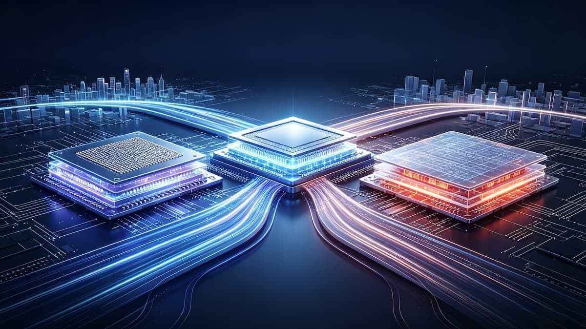
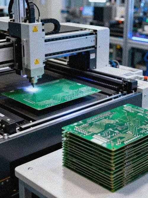
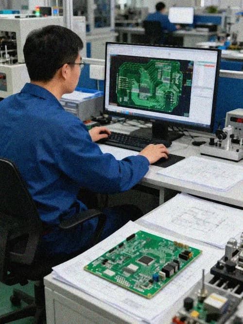
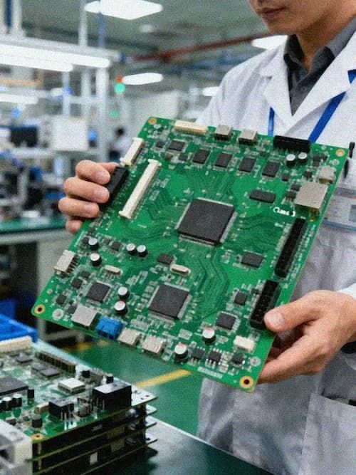
Since TSMC launched CoWoS(Chip on Wafer on Substrate) platform in 2012, advanced packaging has gradually become the core path to continue the growth of semiconductor performance. CoWoS integrates multiple computing chips with HBM(High Bandwidth Memory) high-bandwidth storage through a silicon interposer, which solves the performance bottleneck after the single-chip process is scaled down. Before CoWoS appeared, the semiconductor industry mainly relied on traditional packaging methods such as Wire Bonding and Flip Chip, which gradually exposed the limitations of insufficient bandwidth and high delay in the face of multi-chip integration and high I/O density. In the following ten years, CoWoS architecture evolved from CoWoS-S to CoWoS-L, CoWoS-R, and then to COUPE on Substrate, and the technical route continued to differentiate. On the surface, these differences are differences in packaging forms, which essentially reflect the different trade-offs between cost, performance and manufacturability of advanced packaging. The silicon interposer solution occupies the mainstream with mature industrial chain and stable yield, while the de-interposer solution attracts more and more attention with lower cost and thinner packaging thickness. The two routes put forward completely different requirements on the number of layers, line width, line spacing and size specifications of ABF carrier board at the supply chain level, which triggered the shunt effect on PCB and carrier board. Understanding the technical differences and supply chain effects of these two routes will help to grasp the positioning changes of PCB industry in the wave of advanced packaging.
silicon interlayer route: capacity expansion and carrier consumption of CoWoS
CoWoS-S adopts standard silicon interlayer and conventional ABF carrier board, the number of layers is usually 2 to 4, the line width and line spacing are at the conventional level, and the carrier board area is generally below 55mm×55mm, which belongs to the category of ABF carrier board with relatively basic specifications, and the manufacturing difficulty and cost are within the controllable range. CoWoS-L turns to silicon interlayer with larger size, corresponding to the expansion of ABF carrier board area to 65mm×65mm or even larger, which puts forward higher requirements for warping control and large-size processing. The unit price and manufacturing difficulty of this kind of carrier board are obviously higher than the standard products used by CoWoS-S, and the yield of large-size carrier board is usually 5 to 10 percentage points lower than the standard size, further aggravating the supply shortage. CoWoS-R introduced the silicon bridge and RDL(Redistribution Layer) scheme, and replaced some functions of the interposer with high-density rewiring, which put forward a new standard for the RDL compatibility of the carrier board. In this scheme, the carrier board began to undertake the task of partial signal redistribution, and the functional orientation evolved from simple mechanical support to electrical interconnection assistance, and the number of layers and density requirements increased accordingly. CoWoS-R's carrier board usually needs to support finer lines and more complex power distribution network to match the high-density I/O output of silicon bridge.
TSMC's capacity planning shows that the monthly capacity of CoWoS is expected to reach 75,000 pieces by the end of 2025, nearly double that of 2024, and the goal of 80,000 pieces per month originally planned for 2026 has also been reached before the end of 2025. This pace of production expansion reflects that the AI computing power market is increasingly dependent on advanced packaging. GPU in NVIDIA, self-developed ASIC in Google and Amazon all adopt CoWoS packaging in large quantities, and the consumption of upstream ABF carrier boards increases sharply. It is estimated that each CoWoS package consumes about 0.3 to 0.5 ABF boards. Based on the current production capacity of 75,000 boards/month, the monthly consumption of TSMC alone is between 22,500 and 37,500 boards. This figure does not include similar consumption of other packaging manufacturers such as Samsung and Intel. The rapid climbing of production capacity makes ABF carrier plate one of the weakest links in the whole advanced packaging supply chain, and the delivery cycle is extended from normal 4 to 6 weeks to 12 to 16 weeks, and some high-end specifications are even longer.
Route to Intermediate Layer: How COUPE on Substrate Redefines Carrier Board
Coupon substrate represents a more radical technical direction, which integrates the chip directly on the carrier board and omits the silicon interlayer to reduce the cost and package thickness. TSMC's exploration on this route shows that the scheme of removing the interposer can reduce the total package thickness by about 30%, and at the same time reduce the additional thermal resistance caused by the silicon interposer, which is obviously attractive to mobile devices and thin servers with limited space. In addition, removing the silicon interlayer also means saving the manufacturing cost and integration process of the silicon wafer itself, which can theoretically reduce the total packaging cost by 15% to 20%. This economic incentive is pushing more customers to evaluate the feasibility of this route. However, this route puts forward an unprecedented standard for the wiring density and material properties of the carrier board. The tasks of high-speed signal routing and power distribution, which were originally completed by the silicon interposer, now need to be directly undertaken by the ABF carrier board, so the interconnection density of the carrier board needs to be increased by an order of magnitude, from hundreds of lines per square centimeter to thousands.
ABF carrier board is developing to a larger size, the design of 10×10cm is gradually increasing, and the number of layers is also advancing to more than 14 layers to adapt to the complex interconnection of 3D stacked packages. According to the forecast of industry research institutions, the market scale of ABF carrier board is rising at a compound annual growth rate of nearly 28.8%, and the gap between supply and demand is particularly prominent in high-end categories with high-rise number, thin line width and large size. The manufacturing of high-end ABF carrier boards is highly concentrated in a few suppliers, such as Xinxing Electronics, Yifei Electric, South Asia Circuit, etc. It usually takes 18 to 24 months to build new capacity. The equipment delivery and process debugging further lengthen the supply response time, so the mismatch between supply and demand has a significant lag. In the scheme of removing the intermediary layer, the strategic importance of carrier board has further increased, from the packaging base to the functional layer, and its value has also increased from the traditional 10% to 15% to 25% to 30% of the whole packaging cost, and the bargaining power of carrier board manufacturers in the supply chain has been enhanced accordingly. The proportion of customers signing long-term supply agreements with carrier plants is increasing to ensure the capacity lock-in in the next two to three years.
Divergent effect of two routes on PCB supply chain
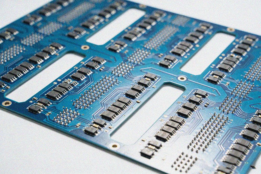
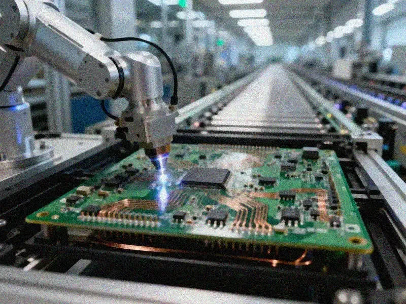
There are obvious differences between the silicon interposer route and the de-interposer route in the specifications of the carrier board and PCB, which are reshaping the participation threshold and competition pattern of the supply chain. In CoWoS-S and CoWoS-L schemes, ABF carrier board mainly undertakes the basic electrical connection and mechanical support functions, and the number of layers is concentrated in 2-4 layers, with relatively loose line width and line spacing, and the technical threshold for PCB manufacturers to extend to this field is relatively low. Some manufacturers with high-end HDI or thick copper technology have been able to enter the supply chain through process improvement, especially those who have accumulated mSAP experience in RF modules and 5G communication equipment, so it is more feasible to transform into low-level ABF carrier boards. The manufacturing process of this kind of carrier board has much in common with high-end PCB, and the subtractive method or semi-additive process method can be applied. The surface treatment is mainly ENIG, and the AOI detection accuracy is required to be in the order of tens of microns. The conventional PCB production line can be competent after moderate transformation, the investment scale is relatively controllable, and the yield climbing cycle is also short.
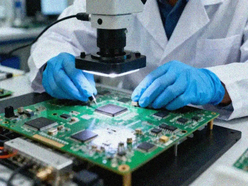
COUPE on Substrate puts the function of the carrier board ahead, requiring the carrier board to directly carry the high-density interconnection originally completed by silicon interlayer, with the line width and line spacing approaching 25/25μm, the warping controlled within 0.1mm, the surface treatment mainly focused on ENIG and ENEPIG, and the AOI detection accuracy reaching micron level. This kind of specification is close to the manufacturing level of IC Substrate, and the conventional PCB production line cannot be directly converted to production. It needs to reach a precise level in cleanliness, temperature control and stress management, and the material selection has also shifted from conventional FR-4 to high TG BT resin with insulating film. This difference blurs the technical boundary between PCB and carrier board, and SLP(Substrate Like PCB) came into being as an intermediate form. Using MSAP (modified semi-additive process) to improve the semi-additive process process, while maintaining the advantages of PCB's large size and low cost, the line width and line spacing level close to the carrier board are realized, which provides a gradual upgrading path for PCB manufacturers and avoids the huge investment and yield risk of direct transition from conventional PCB to IC Substrate.
Technical connection and process threshold of manufacturing end
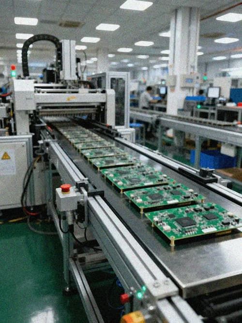
The expansion of advanced packaging capacity is reshaping the boundary between PCB and carrier board, and the process connection at the manufacturing end has become the key to determine whether suppliers can cut into the supply chain. In the silicon interposer route, the carrier board plays the role of the basic platform. Build-up lamination process and conventional reduction method can meet most of the requirements. PCB manufacturers can cut into the supply chain smoothly through SLP technology. The number of product layers is usually between 6 and 10, and the line width can reach 2.0/2.0mil, which can meet the application scenarios of medium density interconnection, and the delivery cycle is relatively short and the flexibility is high. In IC Substrate manufacturing, it is necessary to use BT resin material and insulating film to build a laminated structure. The line width and line spacing in the prototype stage can reach 25/25μm, and it will converge to 30/30μm after mass production, and the impedance control accuracy will be relaxed from 5% to 10%. This gradient difference reflects the comprehensive trade-off between yield, cost and process stability in the process from verification to large-scale production, and also determines the market positioning and customer groups of suppliers in different stages.
The yield climbing cycle of IC Substrate manufacturing is usually as long as 12 to 18 months, and the accumulation of process know-how has significant long-term properties. Enterprises that lay out high TG BT materials and mSAP processes in advance will occupy a favorable position in the next round of capacity expansion cycle. For suppliers with high-end PCB manufacturing foundation, extending to the field of Substrate and SLP is a natural upgrading path. The key success factors include the development of Build-up process, the accumulation of engineering experience of BT materials, and the establishment of joint R&D collaboration mechanism with advanced packaging customers. Global layout and multi-factory collaboration also help to spread the capacity risk and shorten the response period to customers. Under the general trend of multi-source supply chain, suppliers with multiple production bases are more likely to obtain the certification and orders from head customers. KingBrother's long-term accumulation in this field enables it to provide advanced packaging customers with Substrate and SLP manufacturing services from prototype to mass production, covering a wide range of specifications from 2-layer IC Substrate to 10-layer SLP, and continuously invest in process research and development in high-level and thin-line product lines.
Conclusion
Looking forward to the next few years, the technology roadmap of advanced packaging will continue to move towards higher density and lower cost. COUPE on Substrate and other schemes to remove the interlayer are expected to mature gradually, which will push the wiring density of ABF carrier board closer to the level of IC Substrate, and the line width and line spacing may be reduced from the current 25/25μm to below 15/15μm, and the number of carrier boards will also evolve from the current 2-4 to 6-8. The proportion of large-size carrier board will continue to increase, and the design above 10×10cm may become the mainstream specification of AI accelerator packaging, and some ultra-high performance computing chips may even need 12×12cm or more carrier board area. The continuous expansion of AI computing power market will make advanced packaging capacity become the long-term focus of semiconductor industry, the strategic position of upstream carrier board and Substrate manufacturers will also be enhanced, the value distribution of industrial chain is tilting towards materials and equipment, and the joint research and development between packaging plants and carrier board factories will be closer.
For PCB industry, this is a historical window to participate in high-end supply chain, and also a touchstone to test the manufacturing limit. The expansion of advanced packaging capacity is reshaping the boundary between PCB and carrier board, and suppliers who can establish technical connection between the two fields will occupy an irreplaceable position in the global industrial chain. Participants in the supply chain need to be soberly aware that the requirements of advanced packaging for carrier plates are changing from large to small to fine and dense. Only by maintaining a forward-looking layout in process research and development and equipment investment can we gain a continuous voice in this round of industrial transformation. Whether you choose to upgrade gradually through SLP or directly enter the field of IC Substrate, the process accumulation at the manufacturing end and the depth of collaboration at the client end will be the key variables to determine success or failure.