On June 10, TSMC reported consolidated net revenue of NT$416.975 billion for May 2026, up 30.1% from a year earlier. Monthly revenue data from a leading foundry is often treated as an early signal of advanced-node demand because orders for high-performance GPUs, AI ASICs, and networking chips first show up in wafer and advanced packaging utilization before moving downstream into package substrates, PCBs, and system assembly.
Over the past year, most discussions around AI accelerator supply chains have focused on wafers, HBM, and CoWoS capacity. In 2026, another constraint has become harder to ignore: ABF (Ajinomoto Build-up Film) substrates, fine-line organic substrates, and high-density PCBs are carrying more of the design burden in advanced packaging. For procurement and hardware teams, chip availability alone no longer determines whether a project ships on time. Substrate allocation and board-level interconnect schedules can now affect the launch timing of servers, switches, and accelerator cards.
After Wafer Growth, the Pressure Moves to Packaging
Strong advanced-node revenue suggests that AI chip demand remains robust, but high-end chips do not move directly from a fab into system integration. A GPU or AI ASIC must pass through wafer fabrication, advanced packaging, substrate attachment, board assembly, system integration, and reliability testing. A queue in any one of these steps can push schedule pressure downstream.
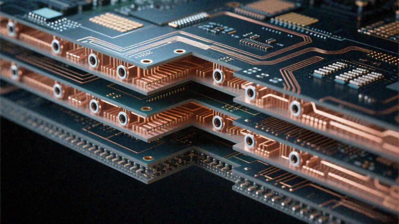
ABF substrates occupy a difficult position in this chain. They sit between the package and the PCB, providing high-density fanout, power delivery, and high-speed signal routing. AI accelerator packages are large, I/O-heavy, and power-dense, which places combined requirements on the substrate: fine lines, multiple build-up layers, low warpage, and high reliability. Process windows used for conventional package substrates cannot simply be transferred to large AI packages because die size, HBM stacks, silicon interposers, and organic substrates expand differently under thermal stress.
Recent generations of AI accelerators have already shown that packaging is no longer a back-end step after chip manufacturing. CoWoS, 2.5D packaging, and chiplet architectures move more interconnect capability into the package itself, and that raises the role of ABF substrates. Substrate suppliers must now manage finer traces, larger body sizes, tighter registration, and lower electrical loss at the same time. When those requirements converge, yield learning often takes longer than equipment installation.
Why ABF Capacity Does Not Scale Quickly
ABF substrate expansion is slow for reasons that go beyond equipment cost. The harder issue is process stability. Large AI package substrates typically require multiple build-up layers and extremely fine traces. Once line and space move into the low-teens micrometer range or below, small variations in exposure, etching, copper plating, and lamination become much more visible in the finished part. Uneven copper thickness can shift impedance, unstable resin flow can create localized voids, and registration drift can weaken microvia reliability.
These problems do not always appear during sample builds. A substrate may pass initial electrical testing, then show microcracking, resistance drift, or open-circuit risk only after reflow, thermal cycling, or sustained power stress. For high-value AI accelerator devices, customers usually require longer reliability programs, including thermal cycling, biased humidity, thermal shock, and board-level bending tests. Even after equipment is installed, a capacity expansion program still needs multiple rounds of material qualification and process-window confirmation.
One package substrate supplier serving North American data center customers encountered yield instability while ramping a large-format AI package substrate. The first pilot lots did not fail primarily through shorts or opens. The issue that slowed the ramp was localized warpage after reflow, which later created insufficient coplanarity at the BGA solder joints. The engineering team traced the problem to thermal stress caused by uneven resin content and copper distribution across the build-up stack. Yield only stabilized after the team rebalanced copper coverage, adjusted the lamination profile, and added intermediate warpage measurement during processing. The ramp took several months, illustrating why ABF capacity cannot be measured simply by counting new production lines.
How PCB Suppliers Are Pulled Into the Constraint
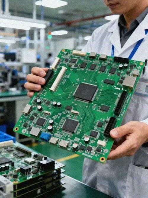
ABF substrates and conventional PCBs are not the same product category, but their worlds are moving closer in equipment, materials, yield management, and customer qualification. AI server motherboards, accelerator cards, OAM modules, and high-speed switch boards are all moving toward higher layer counts, lower loss, and stronger power integrity. When package substrates become constrained, system companies must revisit board-level design because the interconnect density, power path, and heat-spreading capability of the package influence PCB layer count, BGA fanout, VRM placement, and thermal structure.
For advanced PCB manufacturers, this shift creates two types of opportunity. Some suppliers may move directly into package substrates or substrate-like products, extending their processes toward finer traces, higher layer counts, and tighter tolerances. Others will upgrade around AI server and networking boards by using lower-loss materials, heavy copper power layers, controlled backdrilling, precision impedance testing, and stricter warpage management. The first path requires heavier capital investment and longer qualification cycles; the second is closer to existing high-layer-count PCB capability, but still requires better material control and process discipline.
Procurement teams should also understand that ABF substrate tightness does not always appear as a direct price increase from PCB suppliers. More often, it shows up as schedule instability. A packaging delay can push back motherboard BOM freeze; a substrate revision can change BGA pin definitions; a thermal design change can then affect PCB stack-up and copper thickness. A supplier without the engineering capacity to iterate with the customer’s hardware team may still have factory capacity, yet create repeated rework during NPI.
Supplier Evaluation Needs Packaging Awareness
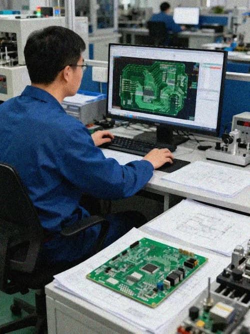
AI hardware supply chains are pushing PCB sourcing toward earlier engineering collaboration. For high-end servers and accelerator cards, PCB suppliers are no longer just receiving Gerber files and building prototypes. They need to help customers identify conflicts among package substrates, connectors, power modules, and thermal components. In OAM, UBB, and high-density switch board designs, BGA escape routing, reference-plane continuity, via structures, and power return paths directly affect signal integrity and production yield.
More capable suppliers are moving DFM, SI/PI simulation, material recommendations, and pilot-build feedback earlier in the design cycle. For example, if an AI accelerator card adopts a larger package body and higher current density, the board shop needs to evaluate whether BGA escape routing will create local copper-density imbalance, whether heavy copper power layers will increase lamination warpage, and whether backdrill depth tolerance is sufficient for high-speed differential channels. If these issues are left until trial production, project schedules can slip by weeks or months.
For global customers, supplier geography also needs to be interpreted carefully. Multi-region manufacturing remains important, but it does not replace process experience. The hard parts of AI accelerator-related PCB and substrate programs are materials, yield, qualification, and engineering response, not geography alone. Suppliers with international delivery experience that can also support high-layer-count fabrication, HDI capability, low-loss materials, and early engineering collaboration are better positioned as advanced packaging capacity expands.
AI Hardware Delivery Is Entering a Substrate-Constrained Phase
TSMC’s monthly revenue growth reflects the continuing strength of AI chip demand, while pressure on ABF substrates and high-density PCBs reveals a manufacturing reality closer to the factory floor. Chip design companies can raise forecasts, foundries can expand advanced-node capacity, and OSAT providers can add CoWoS equipment. If substrate yield, material supply, and customer qualification timelines lag, final system delivery can still stretch out.
Over the next year, AI hardware risk assessment will pay closer attention to packaging and board-level interconnect. Procurement teams need to view ABF substrates, advanced packaging capacity, high-layer-count PCBs, and system assembly on the same delivery map rather than managing them as separate categories. For PCB and PCBA suppliers, customer value will increasingly come from understanding how package changes affect board design, identifying manufacturing failures quickly during pilot builds, and keeping material and process windows consistent across multi-region delivery. As AI accelerators continue moving toward larger packages, higher power, and denser interconnects, these capabilities will sit much closer to the center of supply chain competition.