Overview
Advanced PCB manufacturing is the core foundational support for modern high-performance electronic product R&D and mass production, addressing the growing industry demand for device miniaturization, high-speed data transmission, multi-function integration, and harsh environment adaptability. As electronic systems continue to upgrade, traditional PCB fabrication processes can no longer meet the requirements of high-speed signal stability, high-density routing, and special material compatibility. Advanced PCB manufacturing integrates design optimization, prototyping, quick-turn production, and mass delivery capabilities, following systematic design-oriented logic to help product development teams achieve the optimal balance of product performance, energy efficiency, production cost, and manufacturing cycle, effectively shortening R&D iteration cycles and reducing overall project investment. This manufacturing system covers all mainstream and special PCB categories, adapting to the full lifecycle needs of products from initial prototype verification to large-scale market launch.
Technical Capabilities
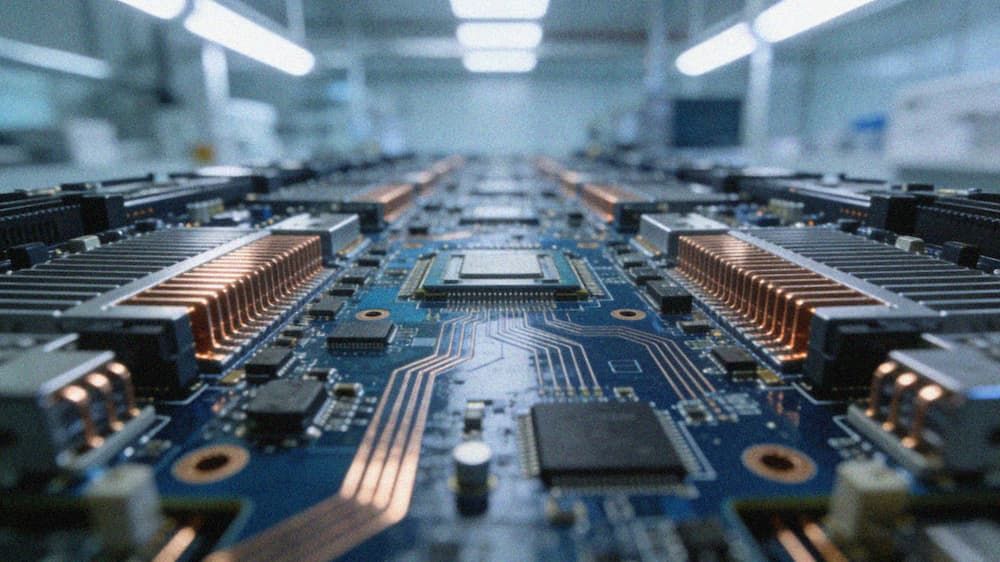
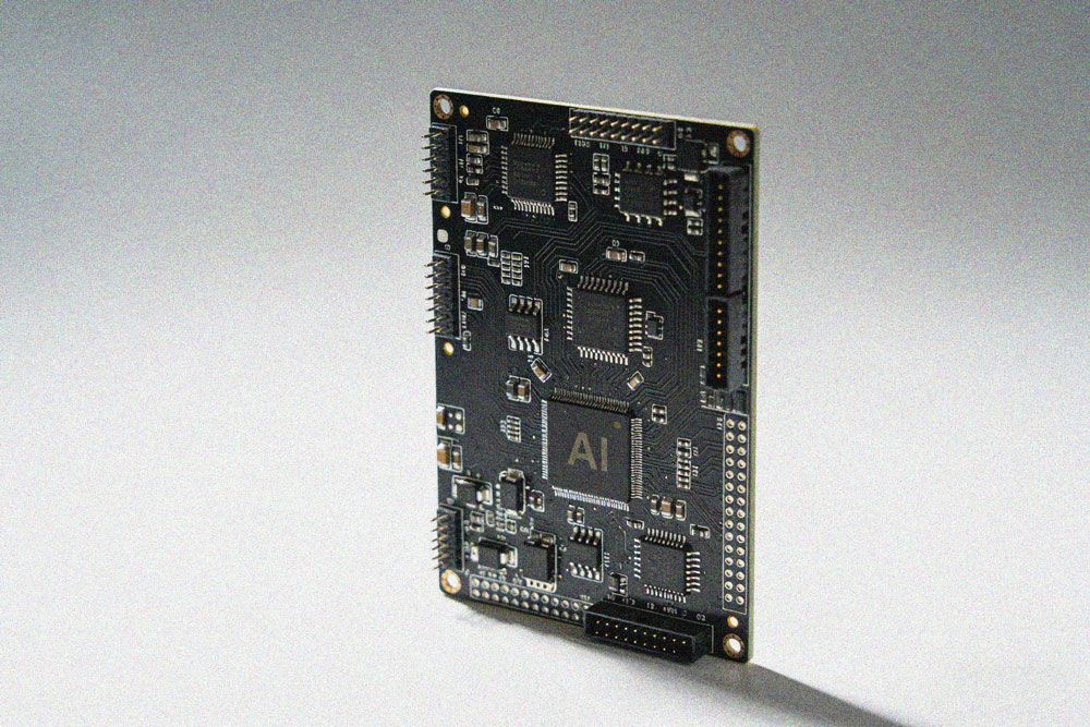
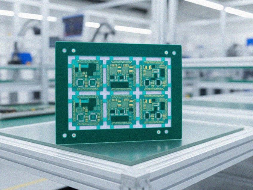
- Full-Category Board Fabrication Support: Covers all common and special PCB types to meet diverse application needs, including single and double-sided boards, multilayer boards, high-frequency step boards, HDI boards, rigid-flex boards, heavy copper boards, high-frequency hybrid boards, mechanical blind buried via boards, metal substrate boards, metal core boards, high-speed backplanes, high-speed optical boards, buried copper block boards, buried ceramic PCBs, ceramic boards, high-resistance carbon oil boards, backlight mini-LED boards, semi-flexible boards, substrate boards, and IC substrate boards.
- High-Precision Process Specifications: Supports minimum 0.5 Pitch component placement, with minimum package size compatibility down to 01005 (0.3mm0.2mm) for ultra-high-density design requirements. Maximum PCB fabrication dimensions reach 600mm450mm, adapting to both compact wearable device boards and large-scale server backplane needs. Component thickness support covers <0.5mm to >3mm, double-sided process device height up to 25mm, and SMD size support for 200mm*125mm and above, meeting special structural design requirements.
- High-Speed Signal Adaptation: Optimized for high-speed signal transmission scenarios, with professional stack design, precise impedance control, and routing optimization capabilities to minimize signal attenuation, crosstalk, and impedance misalignment, ensuring stable transmission of high-bandwidth data for high-performance computing, communication, and intelligent hardware systems.
- Design-Oriented Value-Added Services: Adopts a systematic design-oriented service framework, providing professional PCB design optimization suggestions during the early R&D stage to avoid manufacturing feasibility issues in later stages, helping customers adjust design schemes to achieve the best combination of performance, cost, and delivery cycle.
- Flexible Production Cycle Options: Provides both fast PCB prototype and quick-turn production services for R&D verification stages, with delivery cycles as short as 24 to 72 hours for common prototype demands, and stable, consistent mass production services for volume delivery, ensuring uniform quality between prototype samples and mass-produced products.
Quality Standards
Advanced PCB manufacturing follows strict global industry standards and full-process quality control mechanisms to ensure consistent product performance and reliability. All production links strictly comply with IPC international electronic interconnect standards, and industry-specific standards for automotive, medical, aerospace, and communication fields can be adapted according to project requirements. The quality control system covers incoming material inspection, in-process quality monitoring for each production step, and post-production multi-dimensional verification, including electrical performance testing, signal integrity testing, thermal performance testing, environmental reliability testing (high and low temperature cycle, humidity resistance, vibration resistance), and dimensional accuracy testing. For special material and complex structure PCBs, targeted testing schemes are developed to eliminate potential defects before delivery, ensuring that products meet long-term stable operation requirements in various application scenarios.
Applications
Advanced PCB manufacturing solutions are widely applicable to all electronic industry verticals, including but not limited to the following scenarios:
- **Communication Industry: 5G/6G base station boards, high-speed router backplanes, optical module PCBs, server high-speed backplanes, and satellite communication module boards
- **Consumer Electronics: Mini LED backlight display boards, high-performance smart terminal mainboards, wearable device flexible boards, and gaming hardware high-speed PCBs
- **Industrial Control: Industrial automation controller boards, power electronic heavy copper boards, industrial sensor module PCBs, and intelligent manufacturing equipment control boards
- **Automotive Electronics: Autonomous driving domain controller boards, smart cockpit core control boards, vehicle communication module PCBs, and new energy vehicle power management boards
- **Medical Devices: High-precision diagnostic equipment PCBs, patient monitoring system boards, medical imaging device circuit boards, and portable medical device rigid-flex boards
- **Semiconductor & Aerospace: IC test substrate boards, aerospace electronic component PCBs, and launch vehicle control system circuit boards
Key Advantages
- **Full-Chain Service Coverage: Integrates design optimization, PCB fabrication, component assembly, and multi-dimensional testing services into one system, eliminating cross-stage communication barriers between different service providers, reducing overall project cost, and shortening delivery cycles by 20% to 30% compared to split service models.
- **High Customization Compatibility: Supports customized fabrication for non-standard specifications, special materials, and complex structural designs, providing targeted process adjustment schemes to meet the special needs of niche application scenarios and innovative product R&D.
- **High Yield Assurance: Mature process flow and optimized production parameter control ensure high yield even for high-density HDI, special material ceramic, and complex rigid-flex boards, reducing production waste and lowering the average unit cost of mass production.
- **Reliability Guarantee: Strict full-process quality control and third-party accredited testing support ensure that products meet strict reliability requirements, adapting to harsh application environments such as -40℃ to +85℃ wide temperature range, high humidity, high vibration, and corrosion.
Contact Information
If you have any advanced PCB manufacturing needs, including prototype development, quick-turn production, mass production delivery, or pre-design feasibility consultation, you can contact the professional technical team for support. We will provide targeted solution recommendations and free pre-project technical evaluation services according to your specific project parameters, application scenarios, and delivery requirements.