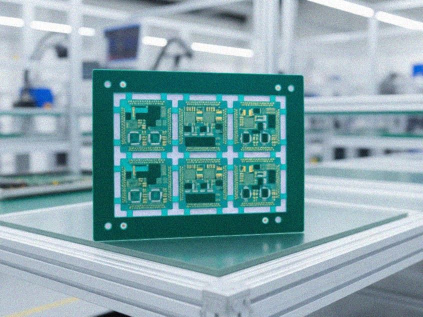
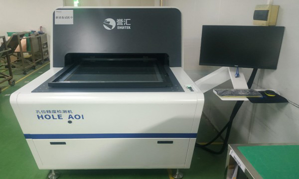
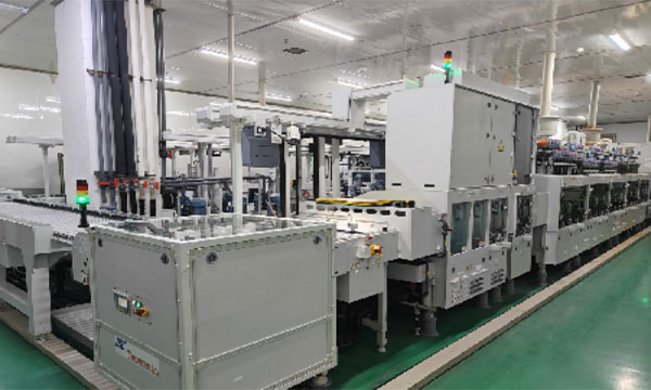
Package Substrate is a carrier used in advanced semiconductor packaging, replacing traditional lead frames to provide conductor support, fixation, heat dissipation, and protection, while enabling electrical connections between the semiconductor and the PCB motherboard. The product uses BT material as the substrate and features microvia technology combined with high-density routing, with line width and spacing up to 30/30 μm, effectively enhancing signal transmission performance and reliability. Package substrates are widely applied in the communications field, including server memory modules and mobile phone storage cards, providing stable and reliable packaging solutions for high-performance electronic products.
Application: Communication; Material: Shengyi SI10US、NBF-T23; Layers / Board Thickness: 6L/0.4 mm; Size: 87.8mm*58mm Line Width / Space: 0.04mm/0.04mm; Minimum Hole Diameter: 0.07mm; Surface Treatment: ENEPIG; Technical Features: MSAP technology with microvia connectivity and arbitrary layer interconnection.