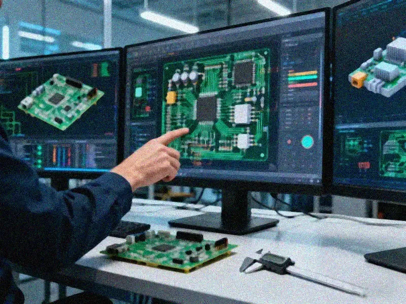
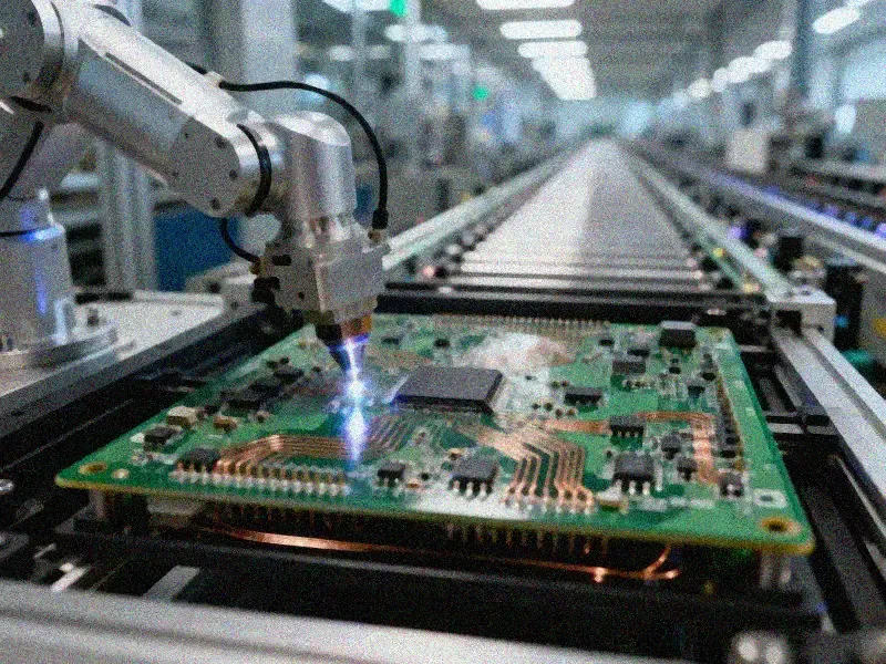
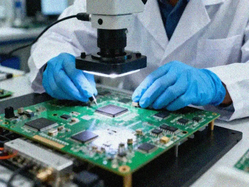
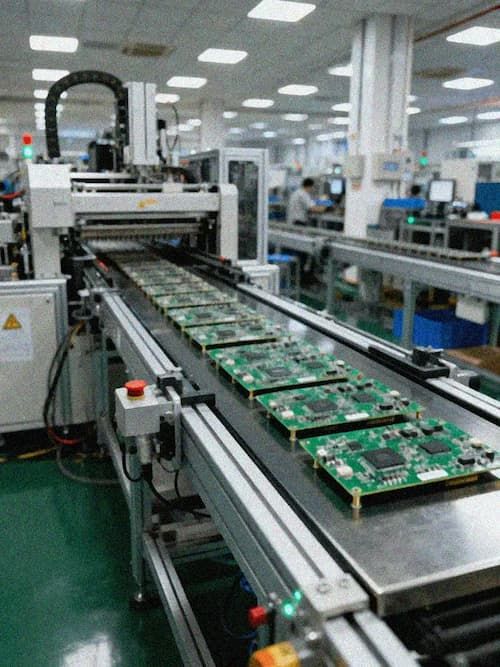
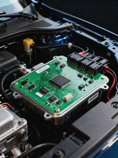
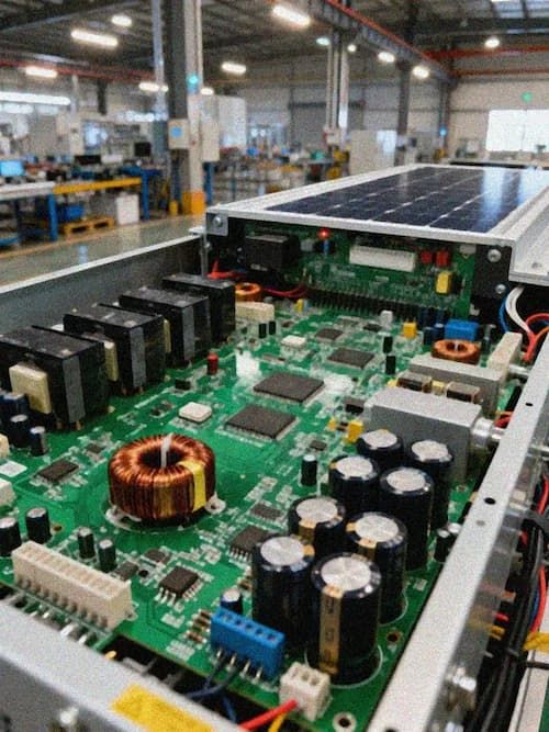
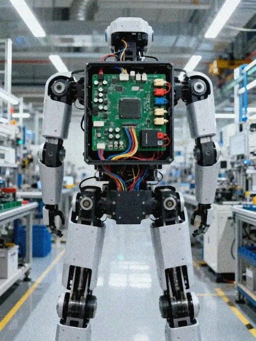
There are three completely different technical directions for PCB design of energy storage systems, corresponding to the three core subsystems of battery management system, power conversion system and energy management system. The BMS side focuses on analog signal acquisition and pursues millivolt accuracy and anti-interference performance; the PCS side focuses on power conversion and handles hundreds of amperes of large currents and heat dissipation; the EMS side focuses on data communication and scheduling algorithms, emphasizing multi-protocol fusion and millisecond-level real-time response. The significant differences in signal characteristics, power levels, communication protocols and environmental tolerance between the three subsystems determine the fundamental division of the PCB design path.
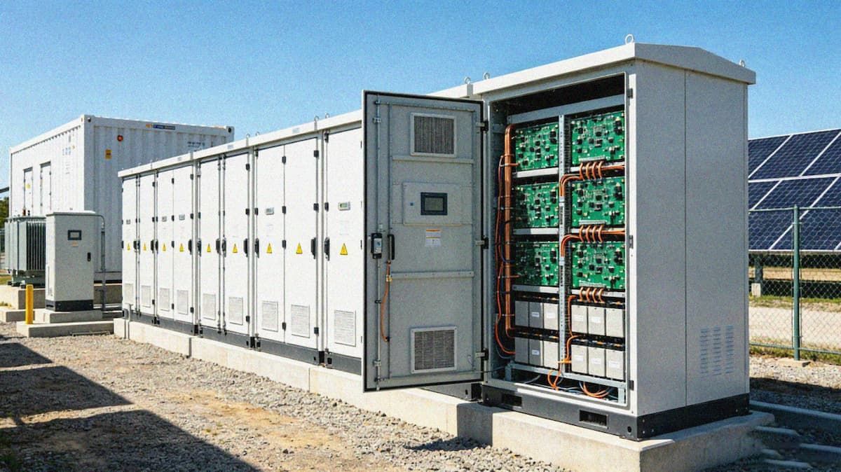
The energy storage system consists of battery packs, BMS, PCS, EMS and other electrical equipment. The three-layer architecture performs its functions. BMS is responsible for battery-level sensing and protection, and continuously monitors individual voltage, temperature and current through high-precision analog front-end chips;PCS completes AC and DC power conversion and grid-side energy throughput, and controls the accurate output of active and reactive power;EMS is responsible for global energy Scheduling and system policy decisions. This functional hierarchy is directly mapped to the design logic of the PCB, and signal accuracy, power density and communication bandwidth become their uncompromising core indicators.
From the perspective of signal characteristics, the voltage signal processed by BMS is usually in the millivolt to volt level and is extremely sensitive to noise; the power signal processed by PCS can reach hundreds of kilowatts, and the parasitic inductance on the current path will directly affect the conversion efficiency;EMS processes It is a high-speed digital communication signal, and the timing tolerance requirements of the PHY layer and protocol stack are strict. The three signals coexist in the same energy storage cabin. Electromagnetic compatibility design requires overall planning at both the board level and the system level. The shielding failure of any single subsystem may affect the normal operation of other subsystems through conduction or radiation coupling. This coexistence environment of multiple types of signals makes the PCB design of the energy storage system much more complex than that of a single functional device.
The installed capacity of global energy storage continues to rise, and design deviations in individual subsystems may cause cascade failures at the entire station. Current technical difficulties focus on high-voltage insulation isolation, wide temperature range material selection and board-level electromagnetic compatibility for multi-protocol communications. In large-scale energy storage power stations, sampling errors in BMS, heat dissipation failure in PCS, or communication interruption in EMS may all lead to serious safety incidents. Therefore, the PCB design of each subsystem needs to establish an independent reliability evaluation system. The differentiated design of the three systems reflects the deep contradiction in energy storage integration.
The BMS high-voltage control board is the first line of defense for battery safety. The core of its design lies in high-precision acquisition and rapid protection response. A typical BMS control board adopts a four-layer layered isolation architecture. The signal layer, power layer, ground layer and shielding layer perform their respective functions, and common mode noise is suppressed through a reasonable stack design. In the layout of the AFE chip, the analog input channel needs to be far away from the power switch and relay drive loop. The sampling traces are in the form of differential pairs and remain equal in length, and the ground loop area is compressed to a minimum.
The accuracy of voltage and temperature acquisition directly determines the accuracy of battery state estimation and health status. In engineering practice, the SOC estimation error needs to be controlled within 3%, and the thermal runaway warning response time needs to be controlled within 10 milliseconds. These indicators put forward extremely high requirements on hardware sampling accuracy. Support measures at the PCB level include using a multi-stage filter network composed of π-type filtering and common-mode inductors to suppress high-frequency noise at the AFE input; optimizing impedance matching to reduce signal reflections; and integrating self-diagnosis pins at key sampling points to achieve rapid fault location. For large energy storage systems with a voltage level of 1500V, isolation withstand voltage design has become a safety threshold that cannot be ignored for BMS boards.
Thermal management cannot be ignored in BMS design. Overcharge, overdischarge, short circuit or temperature runaway are the core risks of battery packs. At the hardware level, overvoltage, undervoltage and overcurrent protection circuits need to be integrated, and at the software level, battery abnormalities are identified in advance through redundant algorithms combined with predictive models. In terms of PCB technology, BMS high-voltage control boards usually use thick copper core plates to improve current carrying and heat dissipation performance. The outer layer of copper is more than 5 ounces thick, and the dielectric thickness is controlled between 0.10 and 0.13 mm. Through high-density multilayer lamination technology achieves compact layout.
The core task of PCS is to realize bidirectional AC/DC power conversion. Its PCB design focuses on three main lines: high current carrying, efficient heat dissipation and electromagnetic compatibility. A typical 100-kilowatt energy storage inverter uses a DC bus voltage of 500 to 900 volts. The power device is mainly IGBT or SiC MOSFET, and the switching frequency is usually between a few kHz and tens of kHz. PCBs need to provide low-impedance current paths for power devices while ensuring the integrity and isolation of the gate drive signals. In large-scale energy storage power stations, the DC side voltage of PCS has gradually evolved to 1500V, which puts forward stricter requirements on the insulation spacing and creepage distance of PCB.
At the layout level, the power part and the weak current control part must be strictly divided. The high-current area formed by DC bus capacitors, power modules and output filter inductors requires wide and thick copper traces. Sometimes a high-thermal conductivity copper strip surface lamination process is used to replace traditional PCB traces to reduce conduction losses and thermal resistance. The layout of the gate driving circuit is particularly critical. The trace length from the driving chip to the power device needs to be as short and symmetrical as possible to avoid voltage overshoots and oscillations during the switching process. For a 500-kilowatt energy storage integrated system, the current carrying requirements of the PCS part are higher. The bus current usually exceeds 400 amps. The heat dissipation design needs to ensure that the temperature rise is controlled within 40 degrees Celsius. The choice of air cooling or liquid cooling solutions directly affects the PCB's laminated structure and substrate selection.
EMC designs face a tradeoff between power density and suppression in PCS. A large amount of electromagnetic interference generated by high-frequency switching actions needs to be controlled by means such as shielding, filtering and grounding. The dual-layer protection process combining three-protective coating and nano-coating can protect the power board from long-term stable operation in high salt fog and high humidity environments. In terms of current level, the DC side working current of a 100kW class PCS can reach more than 200 amps, and the bus current of a 500kW class system exceeds 400 amps. The PCB trace width and copper thickness on these large current paths must be accurately calculated to avoid the risk of overheating during long-term operation.
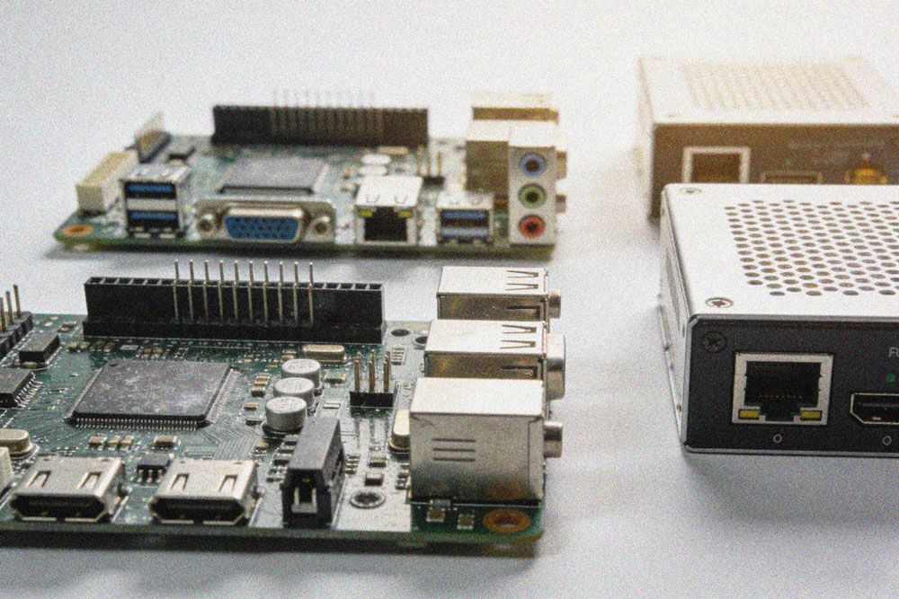
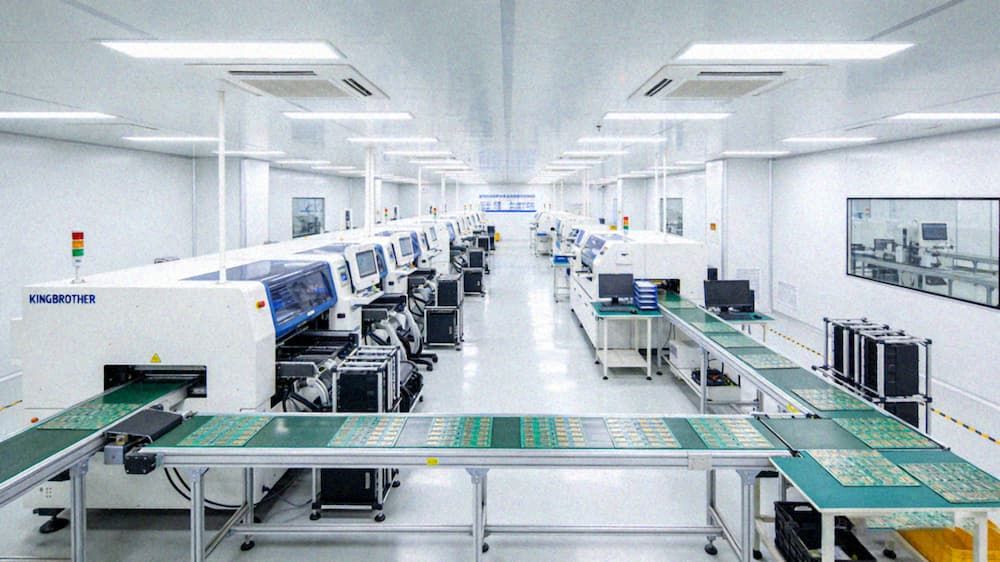
EMS undertakes global scheduling and policy decision-making functions in the energy storage system. The essence of its PCB design is to build a highly reliable multi-protocol communication and computing platform. EMS needs to simultaneously support multiple industrial communication protocols such as EtherCAT, CANopen, Modbus and IEC 61850. Therefore, the board needs to integrate multiple physical layer interfaces such as Ethernet PHY, CAN transceiver and optical transceiver module. Different interfaces have different rates, electrical characteristics and isolation requirements, and PCB layout needs to coordinate the coexistence of high-speed signals, low-speed serial ports and optical isolation areas in a limited space. When manufacturing such multi-interface complex boards, KingBrother usually uses zoning shielding and layered grounding strategies to ensure signal integrity.
FPGA and ARM heterogeneous platforms are widely used in EMS main control boards. The FPGA is responsible for processing high-speed parallel data and hard real-time control logic, and the ARM processor runs Linux or the real-time operating system carries upper-layer applications. The power domain, clock domain and reset strategy of the two chips are different. PCB design needs to provide strict signal integrity guarantees for the DDR4 or DDR5 high-speed storage interface, including impedance control, equal-length routing and power integrity optimization. Driven by the localized supply chain strategy, some EMS main control boards adopt localized FPGA solutions and multi-core ARM SoC solutions, and the autonomy rate of circuit design continues to increase.
The working environment of the EMS main control board is usually located in the control cabinet of the energy storage cabin, and the temperature change range and electromagnetic environment are as complex as the power side. The wide temperature range requirements for industrial-grade chips are generally between minus 40 degrees Celsius and 85 degrees Celsius. PCB materials need to match this temperature range without interlayer delamination or solder joint cracking. In the manufacturing of EMS boards, KingBrother usually selects high-reliability FR-4 materials and ensures the quality of solder joints through an enhanced reflow soldering process. The isolation design of communication interfaces is also crucial. The isolation voltage of Ethernet and CAN bus is usually required to reach more than 2500 V. The selection of optocouplers and digital isolators directly affects the anti-interference performance and long-term reliability of the system.
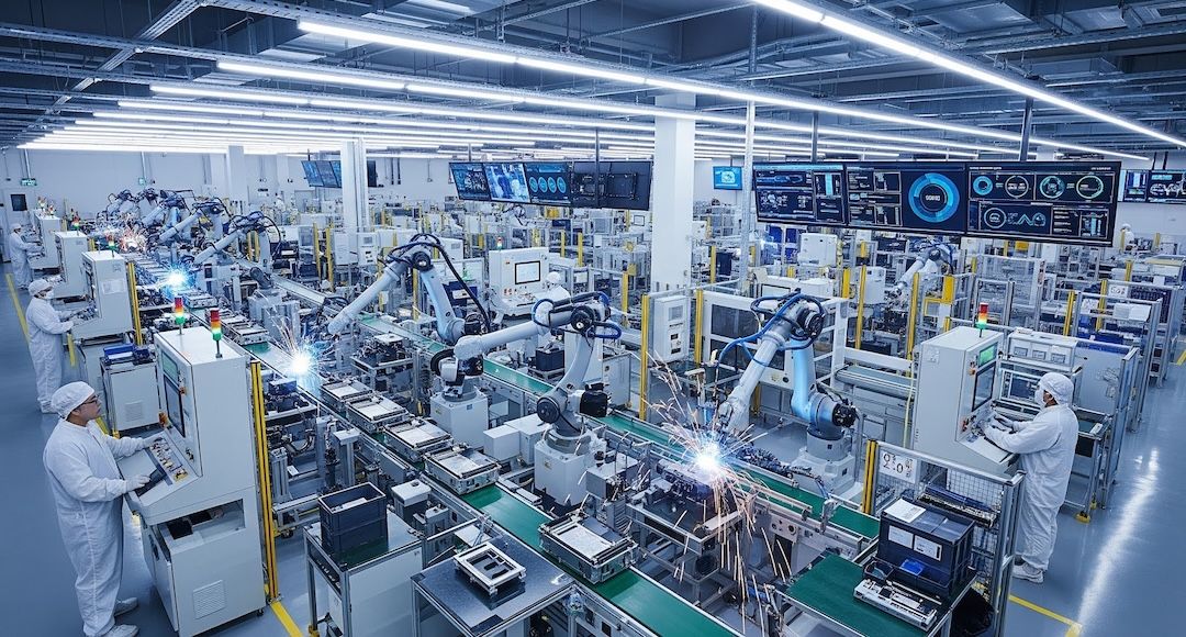
When the three subsystems of BMS, PCS, and EMS are integrated in the same energy storage cabin, the coordination of PCB design becomes particularly important. The unified material management platform can effectively reduce the complexity of the supply chain and avoid manufacturability risks at the design source through a standardized BOM structure and DFM rule base. The process routes of the three subsystems still need to be differentiated: BMS focuses on precision acquisition and small signal processing, PCS focuses on power heat dissipation and high voltage isolation, and EMS focuses on communication processing performance and interface expansion. This differentiation should not become an obstacle to collaboration, but should be organically integrated under a unified quality system and testing standards.
EMC coordination across subsystems is one of the difficulties in integrated design. When the three subsystems are operating in the same cabin, ground level continuity, signal return paths and hierarchical isolation of the grounding system need to be uniformly planned at the system architecture level. The sensitive analog signals of BMS, the high-frequency power noise of PCS and the high-speed digital signals of EMS need to be clearly divided in physical space. The configuration of the shield and filter interface should be determined during the overall design stage, rather than temporarily spliced after each is independently designed.
For energy storage power stations for a 25-year design life, PCB material aging, solder joint reliability and coating durability all need to be fully supported by data during the verification stage. The differentiated design of the three systems reflects the deep contradiction of energy storage integration, that is, coordinating three distinct technical requirements of precision simulation, high-power conversion and high-speed communication in a unified physical space. The degree to which this contradiction is resolved directly determines the overall reliability and operation and maintenance costs of the energy storage system.
The integration trend of energy storage systems is driving the functional boundaries of BMS, PCS, and EMS to blur. Multi-port devices integrate inverter, power conversion and energy management functions into a single cabinet, supporting plug-and-play and millisecond-level energy response, which places higher requirements on the integrated signal, power and communication design of PCB. The popularity of wide-gap semiconductor devices such as SiC and GaN has further forced the upgrade of PCB thermal management solutions. Embedded processes such as ceramic substrate and FR-4 hybrid lamination, buried copper blocks and buried capacitance buried resistors are expected to be used in high-power modules. More widely used.