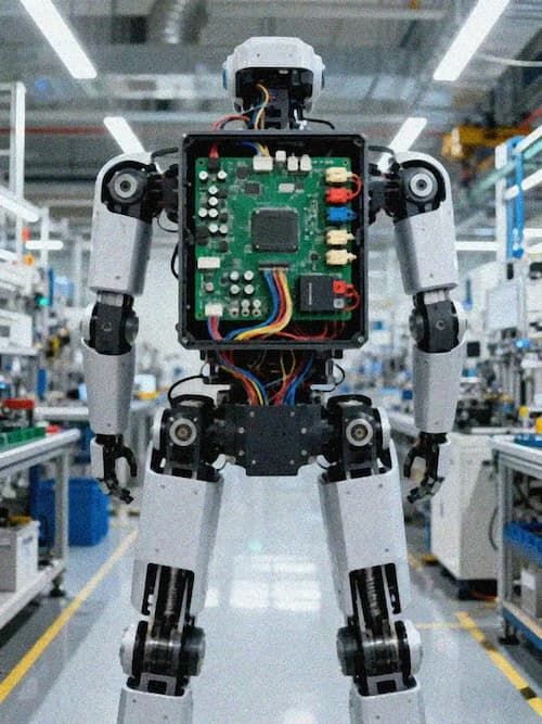
The global power grid is undergoing an unprecedented upgrade
In the past ten years, global installed renewable energy capacity has more than doubled from approximately 1850GW in 2015 to nearly 4200GW in 2024. The proportion of photovoltaics and wind power continues to rise, the access to distributed energy has increased significantly, and the operating model of the power grid is undergoing fundamental changes. Projections from the International Energy Agency (IEA) show that global data center power consumption will double in five years, accounting for 3% of global electricity demand by then. Behind this trend is the deep integration of computing infrastructure and energy infrastructure.
As the core hub connecting the power generation side and the power consumption side, its upgrading and transformation have become a key link in the global energy transformation. According to Prismark data, the global PCB output value in 2025 will reach US$85.152 billion, a year-on-year increase of 15.8%, of which the contribution of the power electronics sector has increased significantly. Every time the voltage level is increased, every energy storage power station is connected to the grid, and every UHV line is put into operation, there are a number of control circuit boards behind them that undertake the functions of signal collection, power driving, and protection execution. These inconspicuous boards form the hardware base for the reliable operation of the power grid.
Ultra-high voltage transmission: an energy highway spanning thousands of kilometers
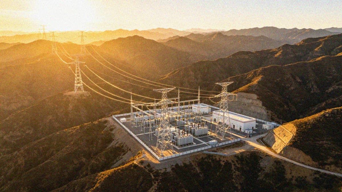
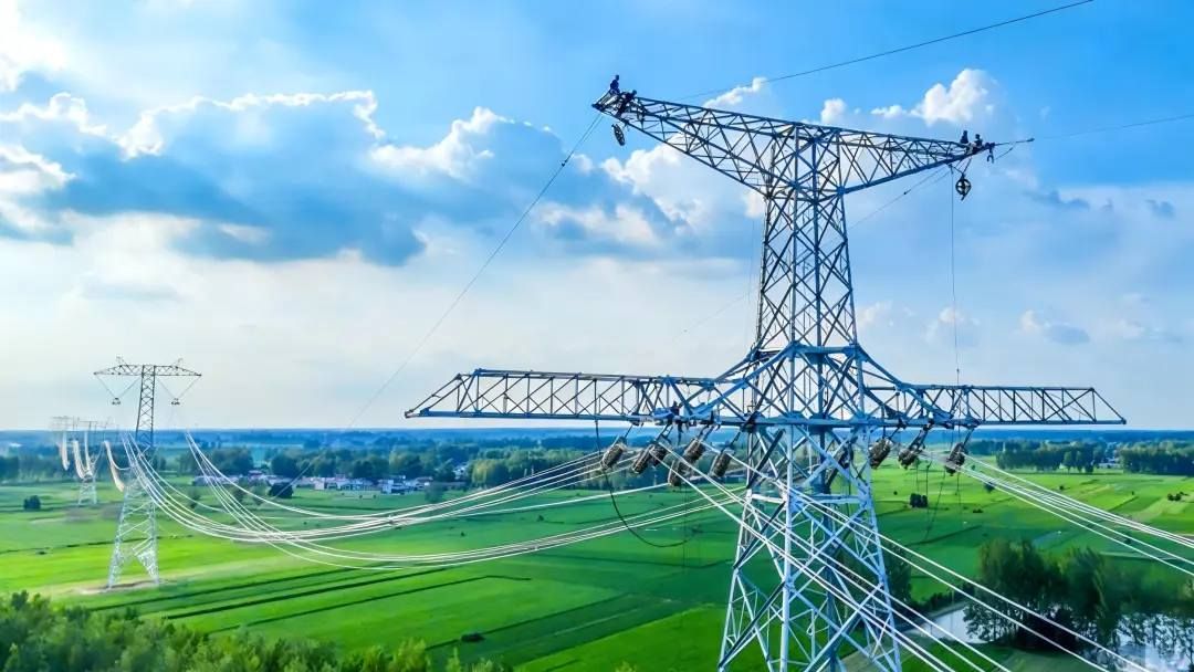
Ultra-high voltage direct current transmission (UHVDC) is the core technology for realizing long-distance, large-capacity and low-loss transmission. An ultra-high voltage DC line of ±1100kV can transition the transmission stage of energy bases thousands of kilometers away with more than 6000MW of power to the load center stage, and the line loss is only about one-third of that of traditional AC transmission. In China, the UHV transmission project has formed the backbone network of "power transmission from west to east." The Baihetan-Zhejiang ± 800kV UHV DC project can transport more than 30 billion kilowatt-hours of clean electricity every year.
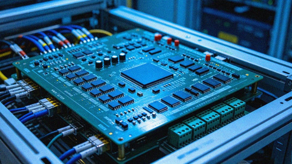
Converter stations are the core link of UHV DC transmission. Among them, converter valves, valve-based electronics (VBE), valve control units and other equipment rely on high-reliability PCBs for precise control. The VBE main control board is responsible for triggering control, overcurrent and overvoltage protection, operating status monitoring and redundancy management of thyristors. Its reliability directly determines the operating stability of the converter valve and even the entire converter station. According to data from the power industry white paper, the rated DC voltage range of HVDC converter valves is ±10kV to ±1100kV, the rated DC current can reach 6250A, the converter capacity can reach up to 5000MW, and the fault current tolerance is up to 63kA.
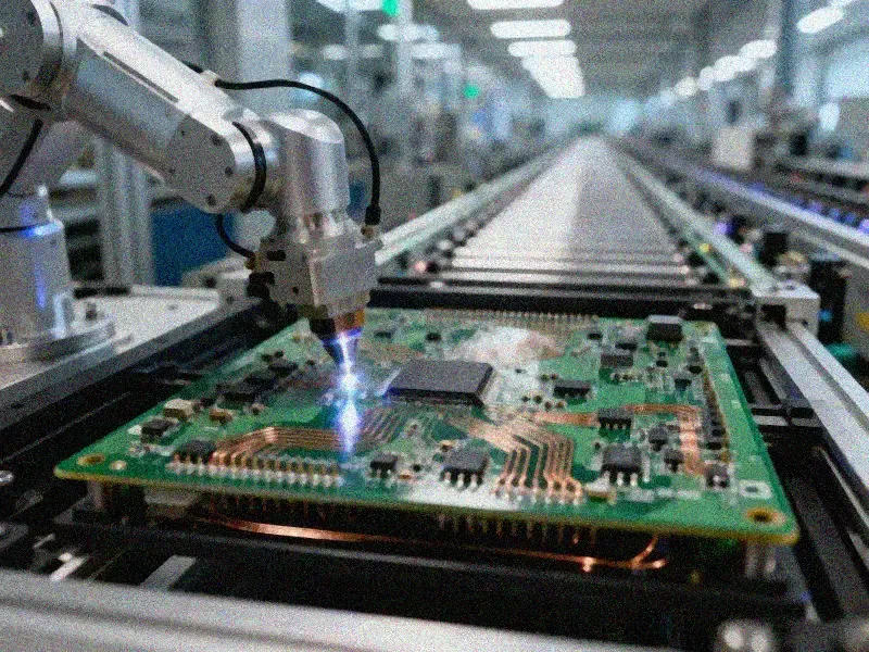
These parameters put forward strict technical requirements for PCBs. The high-voltage transmission plate usually uses halogen-free FR-4 or TG170 and above high glass transition temperature plates. The number of layers is 4 to 10, the plate thickness is 1.6-2.5mm, and the copper thickness is 2OZ. The manufacturing standard must meet IPC CLASS 3. Conventional DC transmission control boards require 12-16-storey TG plates with a minimum line width of 0.05mm to adapt to the operating conditions of ±1100kV voltage level and 6250A current. The pulse distribution board for flexible DC transmission is more complex, requiring a design of 16-24 layers and a board thickness of 3-6 mm. Its performance can be improved by 99%, the yield rate is 100%, and the cost is reduced by 10%.
The operating environment is another challenge. The electromagnetic interference in the valve hall of the converter valve is extremely strong. The environmental temperature is maintained above 50°C for a long time, and the humidity can reach 80%. At the same time, it also faces erosion such as sand and salt fog. The VBE main control board needs to pass high temperature and high humidity aging test (50°C/80%/168h), vibration test (100Hz), 1100kV high-voltage test, and ensure a service life of 25 years. Taken together, these requirements have put forward extremely high thresholds for PCB material selection, layout design, and process control.
Energy storage systems: core support for grid flexibility
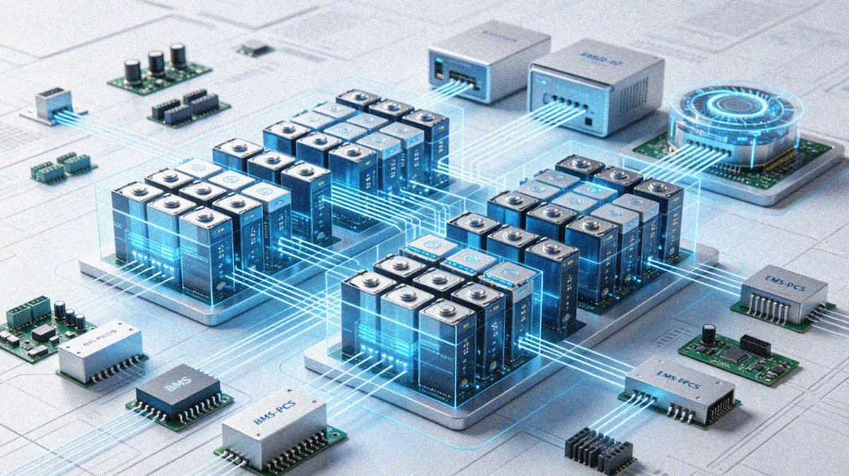
With the increase in the proportion of renewable energy, energy storage systems have become key equipment for peak regulation and frequency regulation of the power grid and stabilizing fluctuations. A complete energy storage system includes three core components: battery management system (BMS), power conversion system (PCS) and energy management system (EMS), each of which relies on a dedicated PCB to realize its functions.
The BMS circuit board is the "sensing center" of the energy storage system, responsible for voltage and temperature sampling of battery cells, state of charge (SOC) estimation, equalization control, and communication with the upper computer. A 500kW/500kWh energy storage system may contain thousands of cells. BMS needs to achieve a millisecond-level sampling response and an error accuracy better than 3%. Thermal runaway warning is a key function of BMS, requiring a response time of ≤10ms and an alarm error of ≤3%. These indicators place strict requirements on the signal integrity, electromagnetic compatibility and long-term reliability of the PCB.
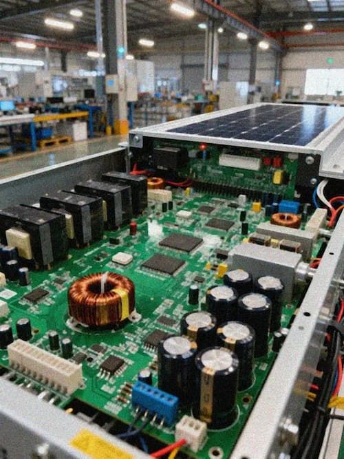
PCS is the interface between the energy storage system and the power grid, and is responsible for DC-AC conversion, power control, and grid-connected/off-grid switching. According to data from the power industry white paper, the bus voltage range of energy storage inverters is 500-900Vdc, and the rated power can reach more than 100KW. The high-power energy storage system adopts a configuration of 500kW/AC380 V/DC800V/500kWh. The PCS circuit board needs to carry high current and achieve high power density, while ensuring a conversion efficiency of up to 98%, and a power factor of ≥0.98. The charging power supply control board usually adopts an 8-12-layer design to achieve 100ms sampling and an accuracy of SOC error of <2%.
EMS is the "brain" of the energy storage system and is responsible for energy scheduling, power prediction, and economic operation optimization. By optimizing the control strategy, the energy storage monitoring EMS board can achieve a performance improvement of 95%, a yield of 100%, and a cost reduction of 10%. In vertical application scenarios, energy storage EMS works in conjunction with wind/photovoltaic inverters, charging power supplies, and microgrid controllers to form a complete energy management network.
Transition from intelligent passive response stage to active prediction stage
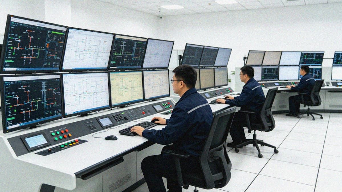
The core features of Smart Grid 2.0's Core 2.0 are real-time monitoring, rapid isolation, proactive prediction and distributed coordination. The traditional power grid operation mode is "response after a fault occurs," while the smart grid requires early warning before a fault occurs, rapid location and isolation after a fault occurs, and minimizing the scope and duration of power outages. This transformation has put forward new requirements for control circuit boards: stronger communication capabilities, higher environmental adaptability, longer service life, and faster response speed.
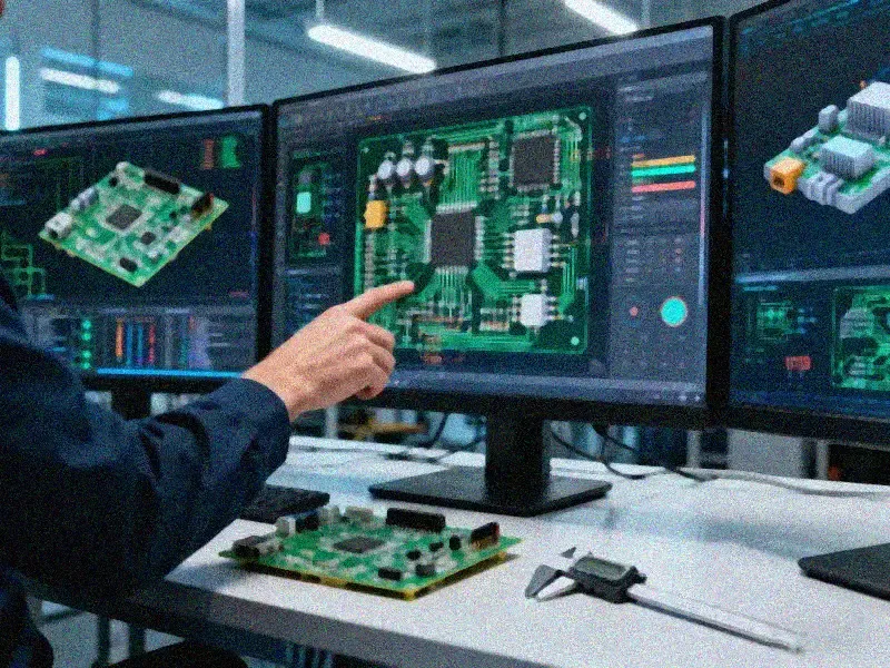
One-stop Hardware Development Services (IPDM) are accelerating the iteration of power grid equipment. IPDM integrates product design (IPD), product management (IPM) and PCB manufacturing, and uses six platforms-IDH design platform, CAD design tool, PCBA assembly platform, component management platform, EES environment simulation platform and P concept stage to transition to the full-process coverage stage of mass production. The KBEDA SKILL tool is based on the Cadence platform and provides more than 400 application functions to support rapid design and verification of power electronic equipment.
In microgrid applications, the IPDM solution has achieved 100% diversification of the device supply chain, which can be discounted at a 30% discount compared with traditional grid electricity prices and reduce costs by 30%. At present, 15 power industry customers including Xidian Power, Xuji Electric, and Gaote Electronics have completed cooperation verification. In terms of quality systems, suppliers must have ISO9001, ISO14001, IATF16949, ISO45001, ISO13485, CQC, UL, ISO/IEC17025 and other standards and certifications to meet the stringent requirements of the power industry.
Hardware infrastructure opportunities for energy transformation
Power grid upgrades put forward three core requirements for circuit board suppliers: in terms of technical capabilities, they need to have mature capabilities in high-TG plate applications, high-multilayer board manufacturing, and special processes (such as hole filling, thick copper); in terms of quality systems, they need to pass the standards and certification of the power industry and have batch consistency control and traceability capabilities; in terms of delivery capabilities, they need to support rapid response and flexible production to adapt to the urgent construction period of power grid projects.
According to Prismark's forecast, global PCB output value will reach approximately US$94.661 billion in 2029, of which the proportion of energy infrastructure will continue to rise. The conventional DC transmission field has created a market value of 11 billion yuan. With the continuous advancement of UHV projects and the rapid growth of energy storage installed capacity, this figure will continue to expand. Suppliers with experience in UHV, energy storage and smart grid delivery have established technical accumulation and customer trust on this track, and market growth in the next five years will flow to these companies.