The core position of BMS circuit boards in new energy vehicles
BMS (Battery Management System) is the core control unit of the new energy vehicle battery system. It is responsible for monitoring the voltage, current and temperature of each cell, and performing functions such as equalization management, charge and discharge control, and safety protection. With the popularization of 800V high-voltage platforms, BMS circuit boards need to simultaneously meet the triple engineering challenges of high-voltage isolation, high-precision sampling and high-reliability operation.
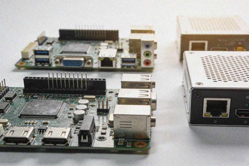
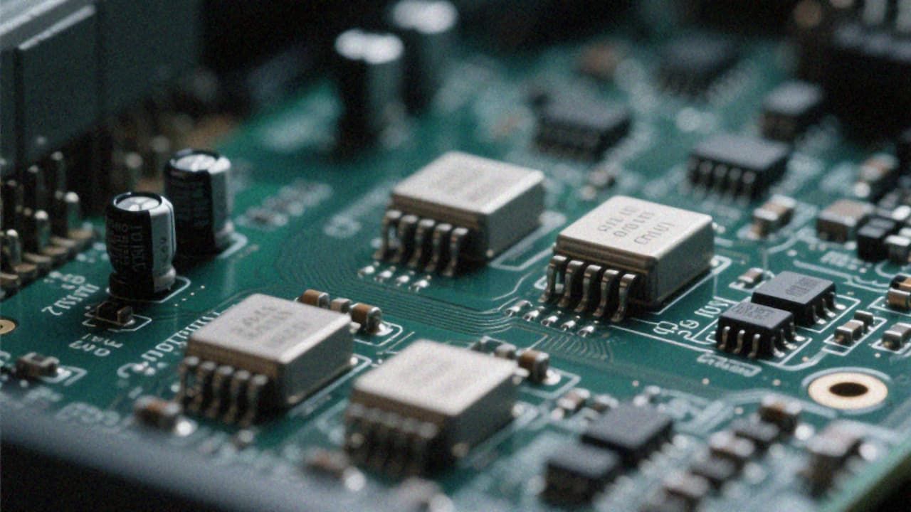
The circuit board architecture of BMS is usually divided into three categories: main control board, slave control board and sampling board. The main control board is responsible for overall system management, communication with the vehicle controller, and execution of charge and discharge strategies; the slave control board is responsible for monitoring and control of battery modules, and each module is usually equipped with a slave control board; the sampling board is responsible for voltage, current, and temperature. The collection of data is the front end for BMS to sense battery status.
High voltage is the primary challenge for BMS circuit boards. The battery voltage of the 800V high-voltage platform can reach more than 800V, and BMS needs to monitor and manage this high-voltage system. The communication between the main control board and the high-voltage system requires electrical isolation, the sampling circuit needs to withstand a high-voltage environment, and insulation monitoring requires continuous detection of the insulation status of the system. These requirements put forward clear requirements for PCB material selection, layout design and process control.
High precision is a core requirement for BMS circuit boards. The equalization management of battery packs relies on accurate voltage sampling, and sampling errors directly affect the equalization effect and battery consistency. Typical voltage sampling accuracy is required to be at the level of ± 1mV. For a battery pack with hundreds of cells in series, the cumulative error in sampling accuracy needs to be controlled within a smaller range. The accuracy of current sampling affects the accuracy of SOC (State of Charge) estimation, and the accuracy of temperature sampling affects the effectiveness of thermal management strategies.
High reliability is a basic requirement for BMS circuit boards. The design life of new energy vehicles is usually 8-10 years, and BMS needs to operate stably within this time span. The working environment of the battery pack has a wide temperature range, vibration and impact persist, and humidity and chemical corrosion (electrolyte evaporation) are also potential risks. Failure of BMS may lead to serious consequences such as battery overcharge, overdischarge, and thermal runaway. The reliability requirements far exceed those of ordinary vehicle-mounted electronics.
KINGBROTHER has been deeply involved in PCB manufacturing for 27 years, serving more than 18000 customers, and holds IATF16949 Automotive Industry Quality System Certification. For teams developing BMS, evaluating suppliers 'thick copper plate manufacturing experience and automotive industry certification qualifications is a pragmatic preparation.
High-voltage safety design points
High-voltage isolation is the foundation of the safety design of BMS circuit boards. The communication between the main control board and the slave control board, and the interface between the sampling circuit and the high-voltage system require electrical isolation. Optocoupler isolation and magnetic coupling isolation are two commonly used solutions, each with its own advantages and disadvantages. Optocoupler isolation has low cost and limited transmission rate and life; magnetic coupling isolation has high transmission rate, long life and high cost.
Creepage distance and clearance are key parameters in high-voltage PCB design. Depending on the operating voltage and pollution level, IEC standards specify minimum creepage distances and clearances. For 800V high-voltage systems, the creepage distance may reach several millimeters or more, which places clear constraints on the PCB layout. KINGBROTHER's PCB manufacturing capabilities cover up to 72 layers (sample)/32 layers (mass production) of FR4, providing a basis for the design of high-voltage PCB.
Insulation monitoring is one of the safety functions of BMS. Determine whether there is an insulation fault in the system by detecting the insulation resistance between the battery pack and the chassis. The insulation monitoring circuit needs to be designed on the high voltage side, and the monitoring results should be transmitted to the main control board on the low voltage side. This transmission process requires electrical isolation while ensuring real-time and reliability of transmission.
Thermal management is an important part of high-pressure safety. Thermal management of battery packs directly affects battery life and safety. BMS needs to monitor cell temperature in real time and implement thermal management strategies. The layout of the temperature sensor needs to consider the thermal distribution of the battery module, and the sampling circuit needs to process multiple temperature signals. KINGBROTHER supports ENEPIG surface treatment, providing a surface treatment foundation for long-term reliability of BMS circuit boards.
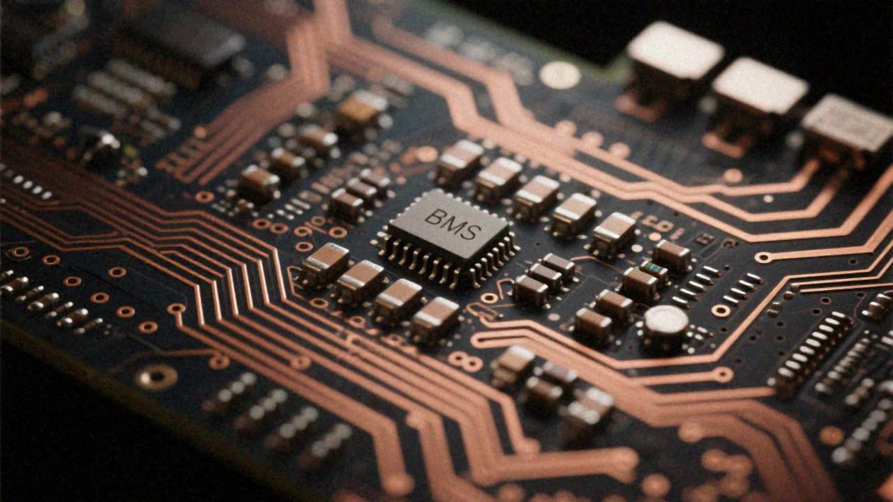
Thick copper design is a typical feature of BMS circuit boards. Current sampling usually adopts a shunt scheme, and large current paths require enough copper foil cross-section to carry current. KINGBROTHER's PCB manufacturing supports a maximum copper thickness of 18OZ (sample)/6OZ (mass production), providing the process foundation for BMS's thick copper design. The design of a 6-layer thick copper BMS board has become a mainstream choice, and the stack design of thick copper layers and signal layers requires careful engineering considerations.

High-precision sampling design
Voltage sampling is a core function of BMS. For a battery pack with hundreds of cells in series, the voltage of each cell needs to be independently sampled. Sampling accuracy directly affects the equalization effect-if the sampling error exceeds the equalization threshold, the equalization strategy may fail. The sampling accuracy requirement of ± 1mV is an engineering challenge for sampling circuits operating in high-voltage environments and subject to electromagnetic interference.
The design points of the voltage sampling circuit include: a differential amplification circuit with high common-mode rejection ratio to suppress the impact of common-mode voltage on sampling accuracy; a precision reference voltage source to provide a stable reference voltage; a low-noise power supply design to avoid coupling of power supply noise to the sampling signal; Shielding and filtering design to suppress electromagnetic interference.
Current sampling usually uses a Hall sensor or shunt scheme. Hall sensors can achieve electrical isolation with limited accuracy and bandwidth; shunts have high accuracy and wide bandwidth, requiring additional isolation measures. The choice of the two options requires weighing factors such as accuracy, isolation, and cost.
Temperature sampling usually uses NTC or PTC thermistors. The number and layout of temperature sensors need to take into account the thermal distribution of the battery module, and each module is usually equipped with multiple temperature monitoring points. Temperature sampling circuits need to process multiple signals while ensuring sampling accuracy and response speed.
KINGBROTHER's PCB manufacturing supports impedance control accuracy of ±5%(sample)/±10%(mass production), and a minimum line width and line spacing of 2.0/2.0mil (sample)/2.5/2.5mil (mass production), providing a process basis for the routing of high-precision sampling circuits. Rogers/M6 high-frequency material and 16-layer HDI design capabilities provide technical support for BMS's high-speed communication interface.
DFM (Design for Manufacturability) is an important consideration for high-precision sampling circuits. KINGBROTHER has established a database of 3.27 million certified materials and 2368 DFM rules, providing data support for material selection and manufacturability design. Selecting proven and mature materials reduces the risk of material-related precision drift.
Thick copper process and high reliability manufacturing
Thick copper process is a manufacturing difficulty for BMS circuit boards. The etching, electroplating, and lamination of thick copper layers require special process control. Excessive etching will lead to thinning of copper foil and affect current carrying capacity; uneven plating will lead to differences in copper thickness and affect impedance consistency; improper lamination parameters will lead to interlayer offset and affect alignment accuracy.
KINGBROTHER supports a maximum copper thickness of 18OZ (sample)/6OZ (mass production), covering the thick copper requirements of BMS mainstream applications. The manufacturing of thick copper plates needs to balance multiple factors such as copper thickness, number of layers, plate thickness, and cost. KINGBROTHER's process experience provides a technical foundation for the BMS team.
Hole filling is a special process requirement for thick copper plates. Vias of thick copper plates require sufficient copper thickness on the hole wall to ensure current carrying capacity. The hole filling process can improve the current carrying capacity of the via and improve heat conduction properties. KINGBROTHER's PCB manufacturing capabilities support the hole fill process and provide process support for BMS's thick copper design.
 Thickening of immersed copper is another process to improve the current carrying capacity of vias. The copper thickness of the hole wall is increased by depositing additional copper on the inner wall of the via. The thickness of the immersed copper needs to control the uniformity to avoid difficulty in solder resistance caused by excessive copper thickness in the hole.
Reliability verification is a necessary step before delivery of BMS circuit boards. The cold and hot impact test simulates the changing operating temperature environment of the battery pack and verifies the thermal cycle reliability of PCB materials and solder joints. Vibration testing simulates the mechanical stress during driving of the vehicle and verifies the mechanical reliability of the PCB and components. The moist heat test simulates a high temperature and high humidity environment to verify the insulation properties and corrosion resistance of the PCB.
KINGBROTHER is equipped with an ISO/IEC17025 certified laboratory that supports functional testing, burn-in testing, and environmental testing, providing a test basis for reliability verification of BMS circuit boards. IATF16949 automotive industry quality system certification, combined with a complete set of certifications such as ISO9001, ISO14001, ISO45001, ISO13485, CQC, UL, and ISO17025, provides a system foundation for BMS compliance.
The engineering difficulties of BMS circuit boards focus on the two directions of thick copper process and high-precision sampling. The realization of 6OZ mass production copper thickness and ± 1mV sampling accuracy requires coordinated advancement from three aspects: material selection, process control, and test and verification. For teams developing the next generation of BMS, selecting a PCB supplier with thick copper plate manufacturing experience and a complete test system is a rhythm arrangement worthy of serious consideration.