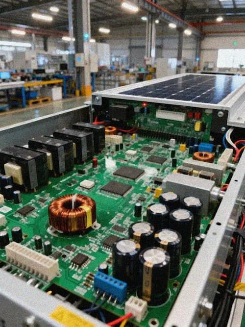
Fatigue effect of high and low temperature cycles on solder joints. How reliable does an industrial control PCB need to be in the factory floor?
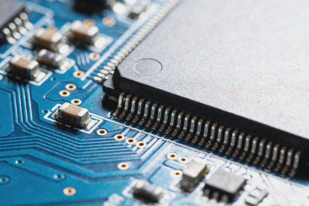
The temperature working range of industrial automation equipment usually requires-40 ° C to +85 ° C, and some outdoor or special scenes (such as metallurgy and glass manufacturing) even require-45 ° C to +125 ° C. The equipment is repeatedly switched between shutdown, start-up, and full-load operation, and the PCB undergoes periodic thermal expansion and contraction. The problem is that the coefficients of thermal expansion (CTE) of PCB substrates, copper foils, solder, and component packaging materials are different. The CTE of ordinary FR-4 plate is about 14 to 16 ppm/°C, the CTE of copper foil is about 17 ppm/°C, and the CTE of BGA solder balls is even higher. When the temperature rises from-40 ° C to +85 ° C, a 200mm×150mm PCB can expand by about 0.4 mm in the length direction. This CTE mismatch applies shear stress to the solder joints during each temperature cycle. After hundreds or even thousands of cycles, microcracks appear in the solder joints and gradually expand, eventually leading to electrical connection failure.
The first line of defense against high and low temperature cycles is plate selection. The glass transition temperature (Tg) of ordinary FR-4 plates is usually 130 to 140°C. The mechanical strength and size stability at the high temperature end are significantly reduced, and the CTE also increases sharply. High Tg plates (Tg above 170°C) maintain better mechanical properties and lower CTE at high temperatures, which can effectively slow down the process of solder joint fatigue. Common high Tg plates include IT180A (Tg 180°C), IS410 (Tg 170°C), etc. The CTE of these plates is controlled at 10 to 14 ppm/°C in the temperature range of-40 ° C to +125 ° C, which is better matched with the CTE of copper foil. In addition, high Tg plates have higher heat resistance and can withstand the higher peak temperature (260°C) of lead-free soldering, and are not prone to defects such as delamination and foaming during the soldering process. Kingbrother has accumulated rich experience in high-Tg plate processing in industrial PCB manufacturing. The conventional plate system covers mainstream high-Tg materials such as IT180A and IS410. It can recommend optimal plate solutions based on the temperature range and CTE requirements of specific application scenarios.
In addition to plate selection, the reliability of solder joints also needs to be guaranteed from the design side. Large-area copper foils should be avoided directly connected to pads, and a thermal relief pad design should be used to reduce thermal stress concentrations. Via holes should be avoided under the solder pads in large-area array packages such as BGA and QFP to prevent solder loss during soldering and resulting in empty solder joints. For applications with stringent temperature cycling requirements, consider using thicker copper foils (such as 2oz or 3oz copper foils) to enhance pad adhesion, or increasing the pad area at critical solder joints to improve the mechanical strength of the solder joints. The laminate design of PCB should also consider symmetry-asymmetric laminate structures are more likely to warp and deform during temperature cycling, increasing solder joint stress.
Connector reliability and structural reinforcement in vibration environments
The vibration environment of industrial automation equipment can be divided into two categories: random vibration and sinusoidal vibration. Random vibration originates from broadband vibration of equipment such as motor operation, compressor operation, and material transportation. The spectrum usually covers 10Hz to 2000Hz, and the acceleration spectral density is between 0.01 and 0.5 g²/Hz, depending on the installation location and equipment type. Sinusoidal vibration comes from periodic excitation of rotating machinery (such as fans, pumps, motors). The frequency is relatively fixed, and the amplitude depends on the mechanical balance accuracy and installation rigidity. PCBs installed in motor drive cabinets, robot bodies, conveyor line controllers, etc. withstand much higher vibration intensity than ordinary industrial PCBs. Failure modes caused by vibration include fatigue fracture of connector pin solder joints, poor contact caused by loose board edge connectors, breakage of internal copper foils caused by PCB warping, and tearing of solder joints of heavy components (such as large capacitors and transformers).
The first line of defense against vibration stress is the mechanical fixation design of the PCB. The industrial control PCB should be installed with four corners fixed or more fixed points, and the fixing screws should use an anti-loosening combination with spring washers to avoid vibration causing the screws to loosen. The fixing holes of the PCB should be positioned as close to the board edge as possible to avoid resonance of the board due to excessive span between the fixing points. For PCBs installed near the vibration source, a shock absorber or silicone buffer layer can be added between the board and the mounting rail to reduce the vibration acceleration transmitted to the PCB. Connector selection is equally critical-industrial PCBs should give priority to connectors with locking mechanisms (such as board-edge connectors with threaded locking or snap-locking locking) to avoid the use of ordinary pins and female that maintain contact only through friction. For scenarios where pluggable connectors must be used, it is recommended to add stress relief designs to the PCB pads of the connector pins (such as lengthening the pads and increasing the copper skin area) to reduce the bending stress suffered by the solder joints.
Conformal coating plays an auxiliary but important role in vibration protection. After the three-protective paint is applied to the surface of the PCB, it can bond the components and the PCB substrate to a certain extent, reduce the relative displacement of the components during vibration, thereby reducing the shear stress suffered by the solder joints. For applications in harsh vibration environments, acrylic three-barrier paints and silicone three-barrier paints are common choices-the former is easy to construct and repair, while the latter has a wider temperature range and better flexibility. Kingbrother provides a complete three-protective paint coating process, supporting three mainstream three-protective paint types: acrylic, silicone, and polyurethane. It can recommend appropriate coating solutions based on the specific vibration and temperature and humidity environment of industrial control equipment. In terms of connector selection, Kingbrother's industrial PCB project experience covers the soldering and assembly processes of a variety of locking connectors. It should be noted that the main function of the three-proof paint is moisture and corrosion prevention, and its protective effect on vibration is limited and cannot replace reasonable mechanical fixing design.
Hierarchical protection strategy in corrosive environments
The sources of corrosive environments in industrial sites are diverse. The air of chemical plants and electroplating workshops is filled with acidic or alkaline gases (such as hydrogen sulfide, sulfur dioxide, ammonia gas). These gases condense on the surface of PCB and form corrosive liquids, accelerating the oxidation and corrosion of copper foils and solder. The salt fog environment in coastal areas poses a serious threat to outdoor installed industrial control equipment (such as port crane controllers and offshore wind power converters)-chloride ions penetrate into solder joints and copper foil surfaces, causing electrochemical corrosion, resulting in solder joints. Increase impedance or even open circuit. In addition, some industrial scenarios also have dust pollution-carbon powder, metal dust, and chemical dust are deposited on the surface of the PCB and form a conductive path in a humid environment, causing short circuits or increased leakage current. The common feature of these corrosion factors is that they act slowly but continuously, and often show obvious symptoms of failure after months or even years of equipment operation.
For different corrosion levels, industrial PCB protection solutions can be divided into three levels. The first level is triple-resistant paint coating, which is suitable for mild to moderately corrosive environments (such as ordinary factory floors). By spraying a protective film of 0.05 to 0.2 mm thick on the PCB surface to isolate moisture and corrosive gases from contact with copper foil. The three-anti-paint solution is low in cost, easy to construct, and has limited coverage of protruding parts such as pins and connectors, and may be penetrated in a highly corrosive environment. The second level is potting, which is suitable for moderate to severe corrosive environments (such as chemical plants and outdoor salt fog environments). The entire PCBA is potted in silicone or epoxy resin to provide comprehensive corrosion protection. The potting scheme has excellent protective effect, but its shortcomings are reduced heat dissipation performance, difficulty in maintenance, and increased weight. The third level is vapor deposition (Parylene coating), which is suitable for extreme corrosive environments (such as offshore platforms and chemical reaction tanks). Chemical vapor deposition forms a uniform and dense parylene film on the surface of the PCB, with a thickness of only 0.01 to 0.05 mm., the highest level of protection, and can withstand the erosion of salt mist, acid mist and organic solvents. Kingbrother provides a complete protection process chain from three-proof paint to potting. Conventional three-proof paint coating supports three types: acrylic, silicone, and polyurethane. The potting process covers two major systems: silicone and epoxy resin, and can be based on the corrosion level of industrial control equipment. Recommended optimal protection plan.
The choice of protection plan needs to be coordinated with the PCB design side. For PCBs using three-proof paint solutions, large areas of exposed copper should be avoided on the board surface (such as grounded copper skin not covered with solder resist) to reduce channels for corrosion intrusion. A masking area needs to be reserved in the connector area to prevent the three-proof lacquer from affecting the contact reliability of the connector. For the potting scheme, PCB design needs to consider the fluidity of the potting material-the spacing between components should not be too small to avoid the potting material being unable to fully fill and form bubbles. In addition, the heat dissipation path of the PCB after potting will change, and the thermal design needs to include the thermal conductivity of the potting material in the calculation. No matter which protection scheme is adopted, the surface treatment process of the PCB should be selected with better corrosion resistance-ENIG (chemical nickel gold) has better corrosion resistance than HASL (spray tin) and should be given priority in corrosive environments.
Electromagnetic interference and PCB-level response in industrial sites
The intensity and density of electromagnetic interference sources in industrial sites far exceed those in commercial and office environments. Frequency converters (VFDs) are one of the most common sources of interference in industrial fields-their IGBT switches switch at high speed at frequencies of tens of kilohertz, producing rich harmonic components that interfere with surrounding equipment through both power lines and radiation. High-power motor drives generate transient large currents and voltage spikes during starting and braking. di/dt can reach thousands of amperes per microsecond. This high-speed current change stimulates a strong electromagnetic field in space. Welding equipment (such as arc welding machines and spot welding machines) generates arc discharges during work, and the radiation spectrum covers tens of kilohertz to hundreds of megahertz, posing a serious threat to nearby control circuits. In addition, the surge voltage generated by relays and contactors in industrial fields when disconnecting inductive loads can reach several kilovolts, which is coupled to the PCB through power lines and signal lines, causing erroneous triggering or even damage to the chip.
To deal with industrial electromagnetic interference, PCB-level EMC design needs to be carried out from three dimensions. Grounding design is the foundation of EMC-industrial PCBs should adopt a complete ground plane design to avoid the ground plane being divided into large areas, resulting in incomplete return paths. For boards where analog and digital circuits coexist, a single-point grounding or section-based grounding scheme should be used to prevent digital noise from being coupled to the analog signal path through the ground loop. Shielding design is an effective means to block radiated interference-sensitive analog signal traces are shielded with ground wires (ground copper skins are laid on both sides), and differential traces are used for high-frequency digital signals to suppress common-mode radiation. The ground plane should be kept intact above and below key chips (such as ADC and communication interface chips) as much as possible, and the mirror image effect of the ground plane should be used to provide shielding. Filtering design is the core of suppressing conducted interference-a π-type filter circuit (LC or CLC structure) is set at the power inlet to suppress differential and common mode interference coupled from the power line; a TVS diode and common mode choke are set at the signal interface to suppress surges and fast transient pulses; Decoupling capacitors (usually a combination of 0.1μF ceramic capacitors and 10μF tantalum capacitors) are placed nearby to the power pins of key chips to provide low-impedance local power supply.
PCB-level EMC designs need to be combined with system-level measures to achieve optimal results. The shielding design of the chassis (metal chassis, EMC sealing gaskets at joints) provides the first electromagnetic barrier for the PCB. The shielding and filtering of cables are equally important-the power and signal lines entering and leaving the chassis should be shielded cables, and the shielding layer should be grounded at 360° at the entrance of the chassis to prevent the cables from becoming antennas for electromagnetic interference. For particularly harsh EMC environments (such as soldering workshops), a metal shield can be installed on the outside of the PCB to enclose the most sensitive circuit modules in a shielded space. System-level grounding design also needs to be coordinated-the working ground of the PCB, the protective ground of the chassis, and the safe ground of the power supply should be connected at a single point at the entrance of the chassis to avoid introducing additional interference from the ground loop. Kingbrother provides PCB-level EMC pre-evaluation services, which can evaluate EMC performance through simulation and actual measurement during the board design stage, identify potential risk points and give optimization suggestions, helping industrial control equipment manufacturers shorten EMC debugging cycles and reduce rectification costs.
Reliability verification system and testing standards
Temperature cycling testing is a core method for verifying the reliability of PCB solder joints. The IEC 60068-2-14 standard specifies the method for temperature cycling testing. Typical test conditions for industrial control PCBs are -40°C to +85°C, with 100 to 500 cycles. Each cycle includes both heating and cooling phases, with a transition time typically not exceeding 15 minutes. The high and low temperature ends are each held for 30 to 60 minutes. After testing, solder joint quality is evaluated through visual inspection, X-ray inspection, and electrical performance testing. Vibration testing is performed according to IEC 60068-2-6 (sinusoidal vibration) and IEC 60068-2-64 (random vibration) standards. Typical vibration test conditions for industrial control PCBs are: random vibration 10 to 500 Hz, acceleration spectral density 0.5 g²/Hz, lasting 2 to 4 hours; sinusoidal vibration 10 to 500 Hz, acceleration 1 to 2 g, sweep rate 1 oct/min, 20 cycles. After testing, connector contact reliability, solder joint cracks, and board structural integrity are checked.
Salt spray testing is performed in accordance with IEC 60068-2-11 and is used to verify the corrosion resistance of PCBs in salt spray environments. Typical testing conditions are a 5% NaCl solution at a temperature of 35°C and continuous spray for 48 to 96 hours. Inspect the corrosion level of copper foils, solder joints and connectors after testing. EMC testing is the most strenuous part of industrial PCB verification and is performed in accordance with the IEC 61000-4 series of standards and covers electrostatic discharge.(IEC 61000-4-2, ±4kV contact/± 8kV air), radiated immunity (IEC 61000-4-3, 10V/m), electrical fast transient pulse train (IEC 61000-4-4, ±4kV), surge (IEC 61000-4-5, ±4kV), conducted immunity (IEC 61000-4-6, 10V) and other test items. As a product standard for programmable controllers, IEC 61131-2 puts forward comprehensive requirements for environmental adaptability, EMC and mechanical strength of industrial control PCBs.
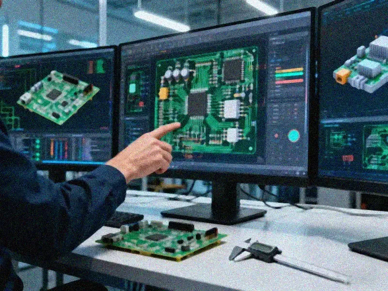
The reliability verification of industrial PCBs should not be carried out after product development is completed, but should run through the entire development process. It is recommended to conduct thermal simulation and modal analysis during the PCB design stage to identify potential reliability risk points in advance; complete the preliminary verification of temperature cycle and vibration tests during the engineering sample stage; complete the formal verification of all test items before mass production and form Test report. For critical application scenarios, it is recommended to conduct accelerated aging tests regularly during the product life cycle to monitor the decline trend of PCB reliability.
Industrial online rate evolves from 99% to 99.9%, PCB reliability becomes the underlying infrastructure
The advancement of Industry 4.0 and intelligent manufacturing is changing the reliability expectations of industrial PCBs. The online requirement for traditional industrial automation equipment is usually around 99%, allowing about 87 hours of downtime per year. The online requirement for smart manufacturing production lines has increased to 99.9% or even 99.99%-the annual allowable downtime has been reduced from 87 hours to 8.7 hours or even 52 minutes. The reliability margin of PCBs needs to be greatly improved. The traditional design-test-delivery process is evolving towards full-life reliability management of design-simulation-accelerated aging-predictive maintenance. The popularity of edge computing nodes and industrial IoT devices has also brought new challenges-these devices are often installed in remote locations with harsher environments and more difficult to maintain. Once a failure occurs, maintenance response times are long and costs are high, and the PCB's "zero-fault" design puts forward higher requirements.
Looking to the future, the reliability design of industrial PCBs will evolve in several directions. In terms of material systems, high Tg plates have changed from optional to standard, and the application proportion of low CTE materials (such as ceramic substrates and metal substrates) in high-end industrial control equipment will continue to increase. In terms of intelligent monitoring, health monitoring circuits on PCBs (such as solder joint resistance monitoring and temperature distribution monitoring) will become a data source for predictive maintenance, helping operation and maintenance personnel intervene in advance before a failure occurs. In terms of design verification methods, digital twin technology will play a greater role in PCB reliability design, replacing some physical tests through virtual simulation and accelerating development iteration. For PCB suppliers, manufacturers with comprehensive capabilities such as high Tg plate processing, three-prevention protection processes, and EMC pre-evaluation will occupy a more favorable position in the supply chain in the Industry 4.0 era.